DESIGN NAVIGATION
Navigation of the design explorer centers around the pins on schematic devices. These provide the common link between a netlist view (looking at all the connections to a pin on a device) and the physical view (looking at all the physical pins on a device). The act of 'drilling down' for closer inspection is both simple and intuitive, making it as easy to interrogate a single connection as it is to examine an entire sheet.
When opened initially (from the Design Explorer command - default shortcut key ALT+X) we are shown a Physical Partslist view of the current sheet as shown below :
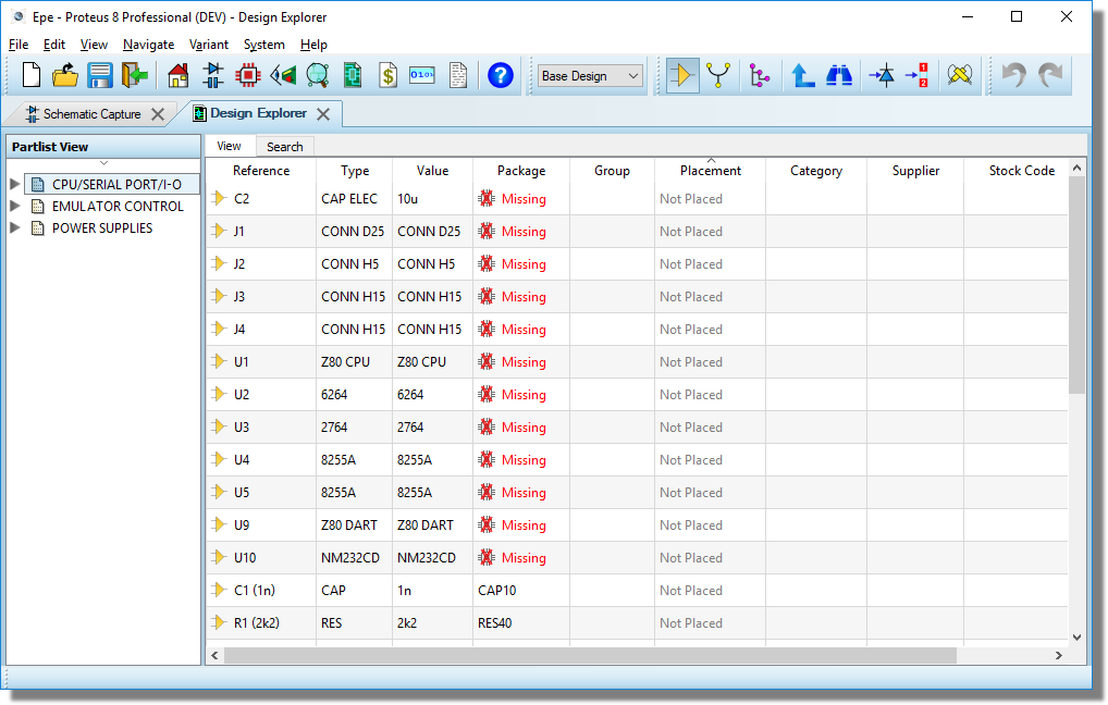
Opening the Design Explorer in Physical Partslist View
The left hand pane shows a list of all the root sheets on the schematic and can be expanded in 'tree like' fashion by clicking on the title of the sheet. On a flat sheet (i.e. one which contains no subsheets) this displays a list of components on the sheet, while in a root sheet which contains a hierarchy (i.e. the sheet contains one or more subsheets) the tree will expand to show the subsheets and root components. The subsheets can themselves then be expanded in the same way, allowing you to quickly and easily navigate through even the most complex of designs.
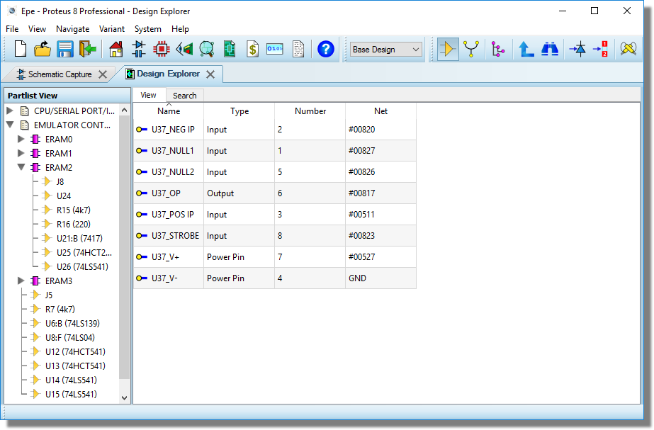
Navigating a multi-sheet hierarchical design in the Design Explorer
The right hand pane provides more information on the components contained in the currently selected sheet or subsheet such as their type, value and packaging. For a sheet containing a hierarchy the child sheets are also displayed in this pane. The contents update as you navigate via the left hand pane and possible errors such as a missing package are highlighted in red.
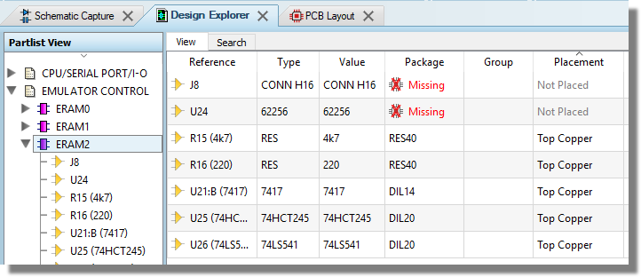
Missing packaged in the Design Explorer
We can drill down even further to look at the pins on a device by clicking on a component part on the left hand pane. When we do this the right hand pane will change to display information on the pins of that component including their electrical type, number and the net on which they are on.
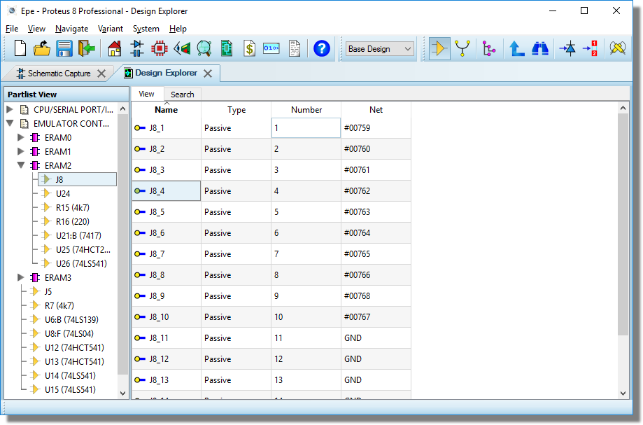
Components are listed on the left hand pane and their associated pins on the right.
The net column will either be a named net (where the net is connected to a terminal or has a wire label on it) or a net of the form #0xxxx. These hash nets simply mean that the net is unnamed and ISIS has therefore designated it a unique identifier. More information on naming nets can be found here.
Having drilled down several levels you can traverse back up the design hierarchy simply by using the up icon at the top of the design explorer.
While we have navigated across and down the schematic hierarchy via the left hand pane, we can also use the right hand pane to navigate 'downwards' from the current view. So, if the current view on the right hand pane contains both subsheets and components a double click on a subsheet will navigate into that sheet (thereby updating the display to show you a list of components inside that sheet) while a double click on a component will update the display to show you a list of the pins on that component.
This is particularly significant where we have a list of pins on the right hand side. No further navigation is possible via the left hand pane (as we have drilled down as far as we can) but a double on a pin on the right hand pane has special meaning. Specifically, it will switch the design explorer into netlist view, displaying the pins net on the left hand pane and all the pins on that net in the right hand pane.
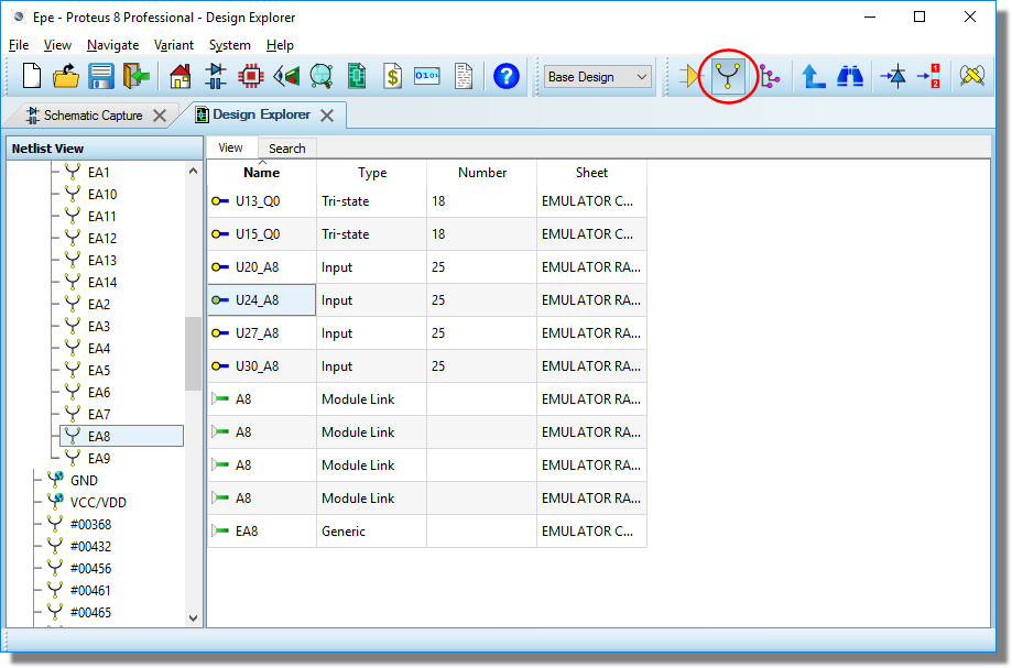
Double clicking on a pin in the right hand pane switches into netlist view and displays all pins on the same net as the actioned pin
This is both extremely clever and extremely powerful, allowing us not only to navigate through a physical design but also to examine the nets and connections on the schematic.
Notice that the left hand pane has updated to display a listing of all the nets on the schematic. Clicking on a net in the left hand pane will show a listing of all the pins on that net in the right hand pane together with information on their electrical type, number and the sheet on which the parent component resides.
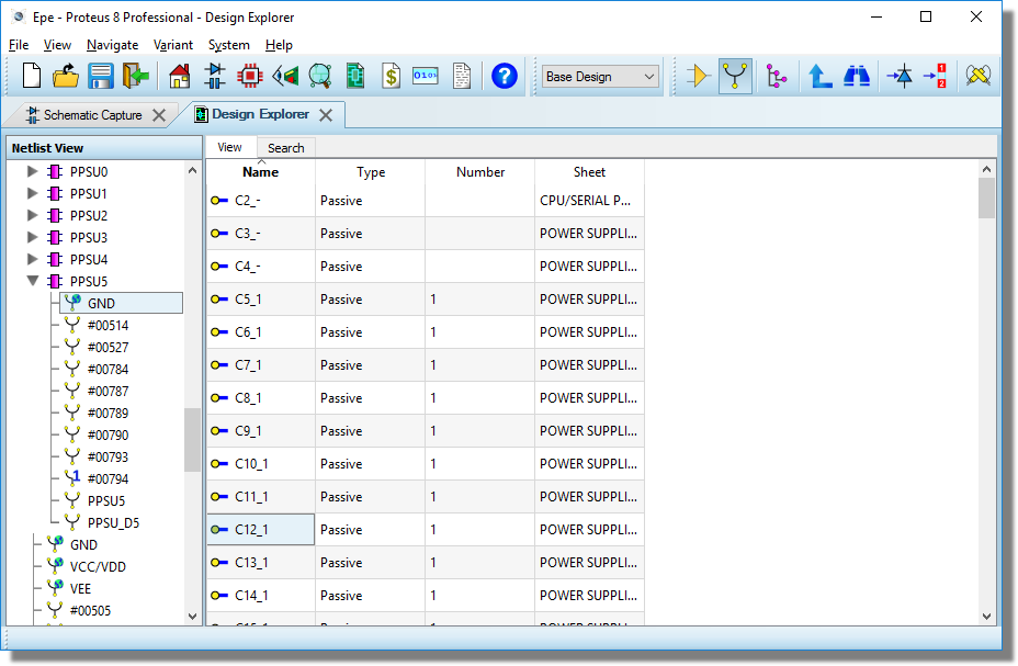
A pin listing for the GND net in the Design Explorer
Finally, double clicking on a pin in netlist view will switch the design explorer back in to partslist view, showing you all the pins on the device that the actioned pin is on.
It follows therefore that we can navigate the design either in Netlist view or in Partslist view to whatever granularity we choose and that actioning pins allows us to seamlessly switch between views. While in this discussion, \we started in Partslist view, drilled down to the pins and then switched to netlist view we can switch to and from netlist and partslist views at any time via the partslist and netlist view icons or their keyboard shortcuts (ALT+P and ALT+N respectively).
Using the Find dialogue to Navigate
To date we have used the windows directly to traverse the schematic but, if we know in advance exactly what we are looking for, we can use the find dialogue to quickly locate it. The Find Dialogue is launched via the find icon on the toolbar at the top of the design explorer and is extremely straightforward to use. For example, below we have configured it to find the VSS net on the schematic.
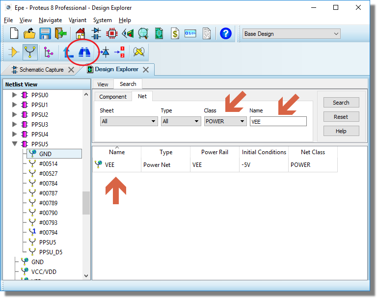
Locating the VSS net via the Find Dialogue in the Design Explorer
The find dialogue form can also be launched from the context menu by right clicking anywhere in the design explorer window or via the CTRL+F shortcut key.
Pin / Label Search
If you need to fins a specific pin or a wire label, you can check the 'Match against Net' check box, set the drop down boxes as required to narrow down the search accordingly, enter the name of the pin or label and click on search:
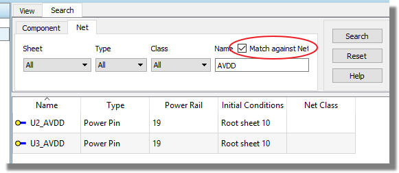
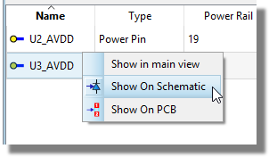
Then you can navigate to the result by right clicking on the net and select your required option: