EXAMPLES
The Design Explorer contains a wealth of functionality as described in the preceding sections. To help clarify the operation of the design explorer the following are some practical examples of the type of things you may do while working on a project.
To check the design for unpackaged parts :
- Launch the Design Explorer in Physical Partslist View.
- Navigate through the sheets via the tree view on the left hand pane.
- Parts without a package will have a red 'missing'' in the package column.
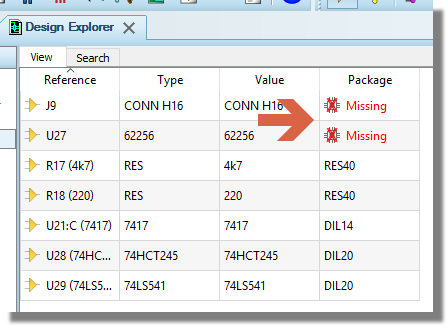
Missing Packages are highlighted in the Design Explorer
To examine one pin nets for possible connectivity errors:
- Launch the Design Explorer and switch to Physical Netlist View.
- All nets on the current sheets will be shown on
the right hand pane. One pin nets are identified both by a separate
icon and by the text 'single pin net' in the Net Type column.
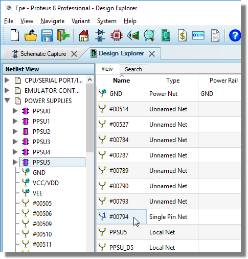
- Right click on a single pin net in the right hand
pane and select goto schematic net from the resulting context menu.
The Design Explorer will minimise and the schematic will zoom in around
the now selected pin which is on the net.
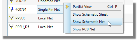
- Click on the Design Explorer in the status bar at the bottom of the desktop to relaunch and repeat step 3 as required.
To highlight the ground net on the current sheet:
- Launch the Design Explorer in ISIS and switch to Physical Netlist View.
- Select the sheet you want to view by navigating through the sheets on the left hand pane.
- Find the GND Net from the list of nets on the right hand pane of the design explorer.
- Right click on the GND Net and select Goto Schematic
Net from the resulting context menu.
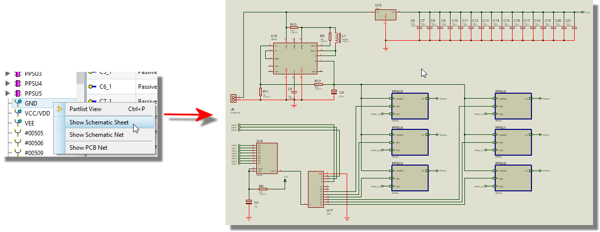
- Repeat steps 2 to 4 as required on different sheets.
To navigate to a nested child sheet on the schematic:
Launch the Design Explorer and then:
either:
- Right click on the selected sheet on the right
hand pane and select the Show Schematic Sheet option from the resulting
context menu.
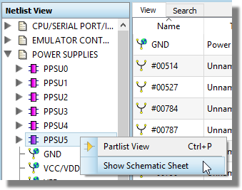
Or:
2. Use the search filter to find components inside a subcircuit / nested child sheet. Select the required sheet from the Sheet drop down list, and leave everything else set to ALL or blank.
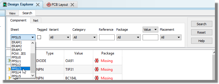
This will list all components on that sheet.
To cross probe to a PCB footprint in ARES
- Make sure that both the schematic and layout applications are open, have the design/layout file loaded and that they are synchronised (that is, that all changes in the schematic have been netlisted through to ARES).
- Launch the Design Explorer in the schematic.
- Make sure that you are in Physical Parts View -
this is shown on the title bar of the design explorer.

- The right hand pane should be displaying a listing
of component parts on the current schematic sheet.
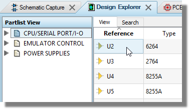
- Right click on the schematic part of interest within
this pane and you should get a context menu with an option to 'Show
PCB Part'. Select this menu option and ARES will both zoom to and
highlight the footprint corresponding to the component you selected.
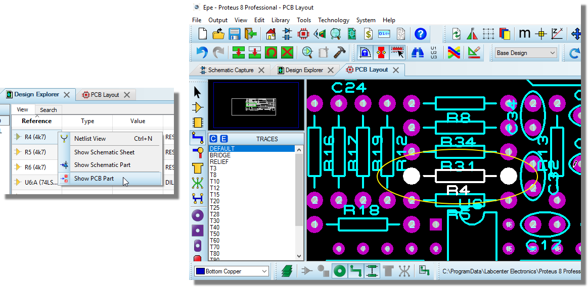
If the 'Show PCB Part' option is grayed out then either ARES is not open, doesn't have the layout corresponding to the open schematic loaded, or the schematic and PCB are out of sync (close design explorer, re-netlist to ARES and repeat from step 2 above).
The Design Explorer is a top level window which means that it can be minimised to the system tray. It will automatically detect when the schematic has changed and will close. This is required to ensure that the information displayed in the design explorer is entirely consistent with that on the schematic.