GUIDED TOUR
When you launch the Design Explorer it will open in a new tab. Like any other module in Proteus 8 you can drag and drop it into free space on your monitor(s) to separate it and create a dual view. Before looking in more detail at the functionality of the Design Explorer we should familiarize ourselves with the window itself. This actually fairly simple and consists of a toolbar and two separate panes.
Toolbar
The toolbar contains eight icons as shown below:

| ICON | DESCRIPTION |
|
This Icon Switches the Design Explorer in to Physical Partslist view. |
|
This Icon Switches the Design Explorer in to Physical Netslist view. |
|
Outline mode opens up the tree so all sheets are visible. |
|
Much like the Windows explorer equivalent, this icon moves the Design Explorer view up a level in the design hierarchy. It is therefore disabled when the view is at root level |
|
This icon launches the a search dialogue form allowing the user to quickly find parts, nets or sheets within the Design Explorer. |
|
This Icon links the design explorer to the Schematic application and allows you to quickly navigate to parts, nets or sheets in the Schematic. The action of the icon is dependant on what is currently selected in the Design Explorer. |
|
This Icon links the design explorer to the PCB application and allows you to quickly navigate to parts, nets or sheets in the layout. The action of the icon is dependant on what is currently selected in the Design Explorer. This icon is only enabled when the layout is open with the corresponding project loaded, and where all changes in the schematic have been netlisted through to the correct layout file. |
|
Live Cross-Probing mode. Best suited to side-by-side viewing setups. |
|
Undo the last design explorer operation |
|
Redo the previous design explorer operation |


Left Hand Pane
The left hand pane of the design explorer is used primarily for navigation. In Partslist View it provides a 'tree-view' of the schematic from root sheets, through hierarchy modules and down to individual components whereas in Netlist View it provides a 'tree-view' listing of all the nets on the schematic. In outline view it will display the sheet hierarchy of the design as a tree view but hide the components inside sheets.
Regardless of which view we are in, it works in the same way as windows explorer (or indeed the contents pane on the left hand side of this help document) where clicking the mouse on an item on the left hand pane causes the right hand pane to update with detailed information on the contents of the item you have clicked on.

The Left hand pane of the Design Explorer in the Partslist View, Netlist View and the Outline View.
Right Hand Pane
The right hand pane of the design explorer provides detailed related to the item selected in the left hand pane. So, for example, selecting a net in the left hand pane (netlist view) will display information on all the pins on that net in the right hand pane and selecting a sheet in the left hand pane (partslist view) will display information on all the components (and potentially child sheets) on that sheet in the right hand pane.
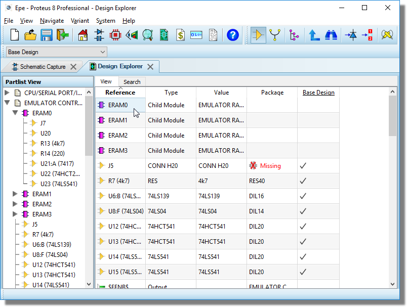
The right hand side of the Design Explorer when opened on a sheet in Partslist View
The information displayed in the right hand pane is dynamic and changes according to what is displayed - this allows us for example to display package information when components are listed in the right hand pane and routing strategies where nets are displayed in the right hand pane.
Icon Identifiers
The design explorer uses several icons to visually identify and distinguish between different items in a listing. These are detailed below :
| ICON | DESCRIPTION |
|
Represents a top level sheet in ISIS. |
|
Represents a Child sheet, Sub-circuit or a hierarchy block in ISIS. |
|
Represents a single component on the schematic. |
|
Represents a single pin on the schematic. |
|
Represents a terminal on the schematic. |
|
Represents a standard net in ISIS. |
|
Represents a net that is design global in ISIS. |
|
Represents a net containing only one pin in ISIS. Note that this is not necessarily an error as a pin in an IC that is unconnected will be identified as a single pin net but may be perfectly legitimate. |


