NETLIST FEATURES
Overview
A netlist is basically the extraction of electrical data from one part of a CAD package into a form that can be interpreted by other parts of the CAD package.
In traditional CAD design, the netlist is created from a schematic and transmitted at the press of a button. This is a batch operation where all of the design changes made are propagated at the same time. By contrast, a live netlist means that individual changes to the schematic are automatically reflected in the other application modules.
Proteus makes extensive use of live netlisting while retaining the option of batch mode netlisting for PCB layout. The schematic capture module generates the netlist and transmits it to the rest of the system. When you make changes to the schematic that affect electrical connectivity (wiring, placement, deletion, etc.) the netlist is also changed in the background and reflected in the other application modules.
The PCB Layout module receives netlist data from the capture module in one of two ways:
- When live netlisting is enabled data is received whenever the layout module is open and visible.
- When live netlisting is off data is received when you manually click on the padlock icon at the bottom of the layout module. The padlock icon will appear when changes to the netlist have occurred (schematic has changed) but have not been received.
Live Netlisting
When live netlisting is on changes made to the schematic will be received by the layout immediately if the layout module is already open and visible or immediately after it is brought to the foreground.
A change that adds to the layout will simply update on the board. For example, the adding of a connection on the schematic will add ratsnest lines on the layout.
A change on the schematic that removes tracks or components from the board requires manual confirmation. Objects which have been removed from the schematic will appear dimmed in the layout and will then be removed entirely when you click on 'changes pending' to synchronise with the schematic. Below is what is seen when the 'Dimmed' colour in Displayed layers is changed to yellow and a component is deleted.
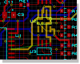
A component deleted on the schematic shown dimmed on the layout, with the Dimmed colour set to yellow
Live Netlisting is on by default, except where a legacy project is imported in which case live netlisting is off by default and must be switched on manually before any editing.
Batch Netlisting
When live netlisting is off a change to the schematic will lock the layout until you manually choose to accept the netlist data. You do this by clicking on the 'out of sync' padlock icon at the bottom of the layout.

The connectivity status reporting Out of Sync
Once the netlist is received you may also have to accept pending changes to the layout if the schematic changes made remove objects already on the board.
The connectivity status reporting Changes Pending
Switching Netlist Modes
When you create a new project live netlisting is enabled by default. You can switch it off with the Live Netlist toggle on the Tools menu.
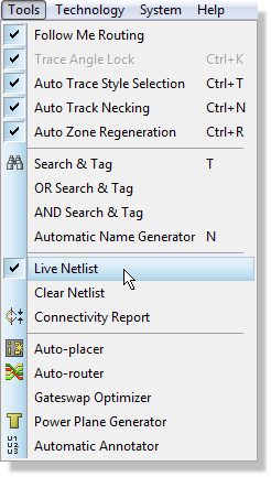
The Live Netlist toggle on the Tools menu of the layout module
Importing from Older Versions
When you import a legacy project from an older version of Proteus live netlisting is switched off by default. You must turn live netlisting on manually with the Live Netlist toggle on the layout module's Tools menu to sync the schematic and layout before doing any further work on the project.
This initial sync will pass the connectivity of the schematic through to the layout and will also bind the parts on the layout to the components on the schematic in the project database.
We do not imagine that anyone would import a semi-complete project but if this does happen note that no components will be available for placement on the layout until you sync (turn the Live Netlist toggle on from the layout module's Tools menu).
We would advise that during development users should work with live netlisting switched on.
The main reason for switching live netlisting off would be on larger layouts with multiple zones where there may be a performance penalty because all of the zone connectivity will be re-calculated on each schematic change. Note however that leaving Live Netlisting On and simply closing the layout tab or frame is just as optimal: netlist updates do not occur in the background.
Netlists and Synchronisation
Communication between schematic and PCB works by synchronising the netlist generated from the schematic with the layout. As described above this can be semi-automatic (live netlisting) or entirely batch mode.
The connectivity status controller in the layout module handles the synchronisation of the board with the schematic. By default, you can find the connectivity status at the bottom of the layout module beside the DRC checker, and it will be in one of seven states at any time.
No Netlist

This is essentially the disabled state and will be shown either when:
- There are no connections in the schematic.
- You have cleared the netlist (Tools menu > Clear Netlist) manually and live netlisting is switched off.
Out of Sync (locked)
The out of sync state is shown only when live netlisting is switched off and the schematic has changes which have not been applied to the PCB. In this state the layout is locked and editing of it is disabled.
Clicking on the padlock icon will apply the current state of the schematic to the layout and the layout will be unlocked for editing. If you have made changes to the schematic that require removal of parts from the layout then you will immediately enter the changes pending state (see below).
If you really need to make a layout change while it is locked then clear the netlist from the Tools menu (return to the no netlist state), make the changes and turn netlisting back on. This shouldn't happen but it is possible.
Changes Pending
This state is shown when the current schematic information has been passed to the layout and there are items which need your confirmation.
You will see this wherever a schematic change involves the removal of object(s) from the layout. The parts and/or tracks in question will dim to illustrate that they are no longer valid and you then have two choices:
- Click on the changes pending button. Proteus asks 'Show or Commit pending netlist changes?' and offers three buttons. Show tags the objects that are due to be removed so that you can see exactly what is affected before you decide; Commit removes them; Cancel leaves the layout in the changes pending state. Once you commit, the dimmed objects will disappear and the schematic and layout will be back in sync.
- Revert the changes on the schematic either manually or via the undo button. Dimmed objects will be re-instated and the schematic and layout will be back in sync
Dimmed objects on the layout awaiting confirmation in the changes pending state
It is worth emphasising that a dimmed object is deemed not present on the board for all but visual purposes. They serve to show the user the effect of committing changes on the schematic and as a placeholder should the user decide to revert changes on the schematic.
If you find that the dimmed devices are hard to see, you can change the colour of the dimming in the Edit Layer Colours/Visibility dialogue form on the View menu (CTRL+L).
Netlist Errors
It is not possible to run a live netlist with errors as the system requires that your netlist is valid. You therefore need to resolve netlist errors as they occur.
If you are working with live netlisting switched off you will need to resolve netlist errors at the point you unlock the layout.
Netlist errors will appear in a separate tab at the point the netlist is transferred from schematic to layout. For example, if you have unconnected power rails you will get netlist errors along the lines of the following:
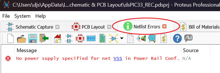
The Netlist Errors tab reporting that no power supply has been specified for the VDD net
Power rails are configured in the schematic module, so you resolve these particular errors there: switch to the schematic and use the Configure Power Rails... command on the Design menu to open the Power Rail Configuration dialogue, then bind each unconnected power net to a supply.
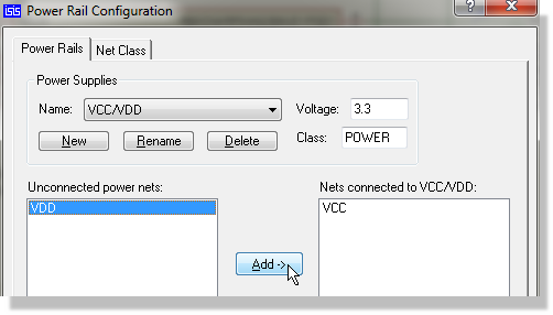
The Power Rail Configuration dialogue in the schematic module, binding the unconnected VDD net to the VCC/VDD supply
See Also:
Power Rail Configuration (Schematic Reference Manual)
No CRC Errors
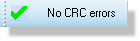
You will see this state whenever a netlist is loaded, the schematic and the layout are in sync and every connection called for by the netlist has been made in copper. In other words, most of the time! The Connectivity Rules Check (CRC) is what compares the two, and this is the state in which it finds nothing to report.
Missing Connections
Where the netlist calls for connections that have not yet been made in copper, the display changes to report how many are outstanding.
Clicking on the widget will launch the Connectivity Errors report, a textual list of the missing connections, and you can navigate to a connection by double clicking on its entry in the list.
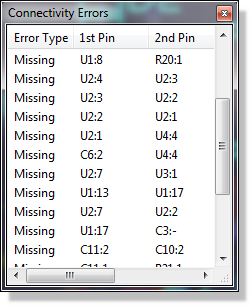
The Connectivity Errors report listing the missing connections on the layout
The same report is available at any time from Tools menu > Connectivity Report. As well as missing connections it lists extra ones, that is copper which joins pins that the netlist does not connect, and the Error Type column tells you which kind each row is. Double click on any entry to navigate to it on the board.
Checking
The status reads 'Checking...' while the connectivity check is running. On a large board with a lot of copper you will see this briefly each time the board changes.
Working with Schematic and Layout
In normal operation you will have a schematic design to associate with the layout. The interaction between the modules is largely intuitive but is detailed in the schematic reference manual (Help menu > Schematic Module). Practical examples also exist in the tutorial documentation.
See Also:
Design Iteration (Schematic Reference Manual)
Netlists and Design Changes (Layout Tutorial)
The Bridge Style and Joining Nets
It is sometimes desired to join nets at a particular point (or points) on the layout, for example where you have an analogue and digital ground and you want to keep the digital return currents off the analogue net. The Proteus layout allows you to do this by creating and using a trace style called the Bridge Style. Simply drag out a track from a pad on net A to a pad on net B using the bridge style.
Any trace style whose name begins with BRIDGE is treated as a bridge style, and the test is not case sensitive. You can therefore keep several separately configured bridges in one design, naming them BRIDGE_GND, BRIDGE_ANALOGUE and so on.
By necessity the bridge style ignores connectivity and DRC conditions (it is after all explicitly used to connect two nets!). It is therefore entirely at the designer's discretion as and when to use this: the software will not warn you if you make a mistake when using this style.
If the Bridge style does not appear in the Object Selector when Trace Mode is selected you can easily create a trace style (Library menu > New Trace Style) and call it BRIDGE.
A bridge track has to ignore the design rules, whereas Follow Me Routing needs them in order to work. Placing a bridge track therefore turns Follow Me Routing off; Proteus tells you when this happens, and you must switch Follow Me Routing back on yourself once the bridge is placed.
Problems with Pin Numbers
As the netlist is loaded, Proteus pulls in the specified package for each component and then attempts to match the pin numbers used for that component in the netlist against the pin numbering in the library-package. If the netlist references a pin number that does not appear in the library package then it displays an error message box and you must click OK to acknowledge. Problems in this area usually arise from one of the following causes:
- Specifying the wrong package, for example a bipolar transistor outline for a regulator.
- Failing to manually number pads which require non numeric 'numbers'. A typical example might be a DIN connector which has pin numbers like A1, A2 etc. Remember that by default, Proteus always numbers the pads in the order you placed them.
- Leaving spaces on the ends of schematic device pin names/numbers or in layout pin numbers. This can be checked by editing the relevant object and examining closely the state of the baseline of the Data Entry Field on which the text sits. If there are any gaps in it, these designate the presence of spaces.
If you use the Packaging Tool in the schematic when creating new library parts, you should avoid any of the above problems.
See Also:
Visual Packaging Tool (Schematic Reference Manual)
Packaging Considerations
At some point during the design process, it is necessary to specify the library-package to be used for each component. With the Proteus system, this can be done:
- At the schematic end by storing the package name in the PACKAGE property. For pre-supplied library parts this is generally done for you, although you can change the footprint if required. For parts you create yourself, you need to add a packaging manually, normally via the Visual Packaging Tool.
- At the layout end as you place the part.
In the latter case, parts without a specified package will appear in the Object Selector in the layout in exactly the same way as those with footprints. When you then try to place the part in the layout you will then be prompted to assign a footprint to the part.
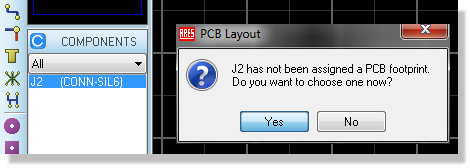
The layout module prompting for a footprint when an unpackaged part is placed
See Also:
Device Libraries (Schematic Reference Manual).
Connectivity Highlight
Connectivity Highlight mode is selected by clicking left on the Connectivity Highlight icon. You can then:
- Highlight/tag a group of pads, tracks and vias connected to a pad by clicking left on the pad.
- Highlight all pads, tracks and vias connected to a net by selecting the required net from the Object Selector and then clicking left on the 'T' toggle.
- Delete all tagged pads, tracks and vias by clicking left on the Delete icon. Combined with the above this provides the means to rip up all tracking associated with a given net.
- Untag all pads/tracks/vias by clicking right at a point where there is no object or else by invoking the Redraw command.
Cross Probing
Proteus provides comprehensive cross-probing directly from within both schematic and layout modules. Inside the layout, you can right click on a footprint to find the component on the schematic or right click on a track to tag the net on the schematic.
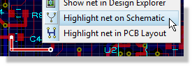
The Highlight net on Schematic command on the layout net context menu
Conversely, on the schematic you can right click on a component or wire to tag the footprint or tracks on the layout.
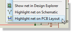
The Highlight net on PCB Layout command on the schematic net context menu
Finally, you can use the Design Explorer module in cross-probing mode to tag both component and footprint in schematic and layout respectively.
If the layout is not synced with the schematic then the cross probing may give very strange results as the layout does not correctly reflect the schematic. Similarly, attempting to cross probe to an unplaced footprint will do nothing as the footprint is not present on the layout.
See Also: