PINSWAP & GATESWAP
Overview
When used in conjunction with the schematic, Proteus layout supports pin-swap/gate-swap changes to the connectivity whilst the layout is being routed. This means that you can choose to interchange the wiring to like pins, and/or interchange the use of like elements of multi-element parts. A full discussion of how to prepare your library parts to exploit this feature is given in the schematic manual, but from the layout side there are two ways of using this feature.
See Also:
Pin Swap / Gate Swap (Schematic Reference Manual)
Gate-Swapping Components on the Schematic (Schematic Reference Manual)
Manual Pin-Swap/Gate-Swap
To perform a manual pin or gate swap
- Select Ratsnest icon.
- Click right on the source pin to bring up the context menu and choose Manual Pinswap/Gateswap. For a gate-swap, the source pin can be any member of the gate. The ratsnest lines connected to the pin will highlight. In addition, legal destination pins will also highlight. The command is greyed out where no legal swap exists for the object you picked.
- Hold down the left mouse button and drag the ratsnest lines to the required destination pin.
- Release the left button. Proteus will make the change, updating the ratsnest and force vectors as appropriate. In the case of a gate-swap, Proteus will move other ratsnest lines automatically.
It is possible to combine a pin-swap and a gate-swap in one operation. For example, swapping input A gate 1 (pin 1) with input B gate 2 (pin 5) on a 7400 will do just this.
Pin-swaps and Gate-swaps constitute changes to the connectivity of your design. Proteus uses the pin-swap and gate-swap data specified in the schematic libraries to decide what is, and is not, a valid swap. If there are errors in this data, then Proteus may well suggest illegal swaps. We will not, under any circumstances, be held liable for any costs incurred or losses arising as result of such mishaps, whether the error be in your library parts or ours or in the software itself. We strongly recommend that you check that the swaps you make are really legal, and that you prototype your PCB prior to the manufacture of large quantities.
Automatic Pin-Swap/Gate-Swap
In the case of a board with a large number of possible gate-swaps (the Shiftpcb sample is a spectacular example) it can be very hard to find the best arrangement. For these cases we have provided an automatic gate-swap optimiser.
To perform automatic gate swap optimisation
- Invoke the Gateswap Optimizer command from the Tools menu and confirm the prompt.
- Proteus will make repeated passes trying the current set of possible swaps. The process repeats until no reduction in ratsnest length is achieved.
- When it finishes, the optimiser reports what it managed, in the form 'Ratsnest reduced by 3.5 inches in 4 passes.'
The Gateswap Optimizer relies entirely on the gate-swap data specified in the schematic component libraries to decide what is, and is not, a valid swap. If there are errors in this data, then the swap optimiser is likely to make erroneous changes to the connectivity of your design. We will not, under any circumstances, be held liable for any costs incurred or losses arising as result of such mishaps, whether the error be in your library parts or ours or in the software itself. We strongly recommend that this command be used only if you are going to prototype your PCB prior to manufacture.
Synchronisation with the Schematic
Whether manual or automatic swaps are to be performed, it is a requirement that the changes can be reflected or 'back-annotated' into the schematic. This will happen automatically provided that your schematic and layout are in sync.
If the layout has not been synced with the schematic the gateswap and pinswap operations will fail as the changes cannot be safely passed back to the schematic. Proteus reports this as 'Pinswap/Gateswap is disabled because schematic has changed!'
A swap that is not among those declared for the part is refused with 'Illegal pinswap! - Legal pinswaps must be specified in ISIS.' Legal swaps come either from the PINSWAP property on the schematic component or, preferably, from the packaging pinout.
Pin-swap and gate-swap are discussed further in the chapter entitled Schematic & Layout in the schematic reference manual.
PINSWAP and Netlist Errors
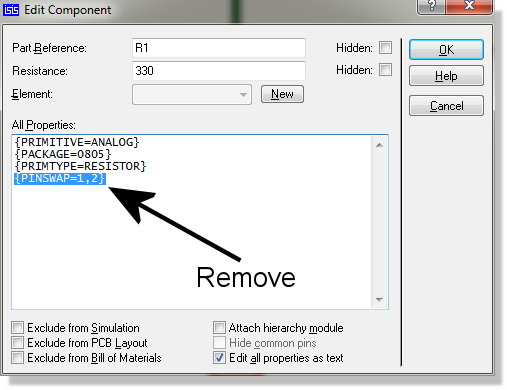
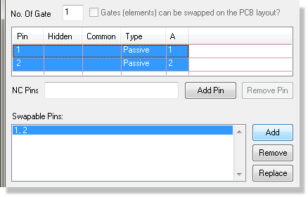
You may occasionally see PINSWAP errors in the netlist. This happens when you have defined swappable pins in two places for one part, namely in the component as a property and in the packaging pinout. This is not resolvable by the netlist and the solution is to remove the ambiguity as follows:
- Remove the PINSWAP property from the schematic component. This is largely enabled for legacy purposes; swappable pins should be defined via the packaging tool.
- Add the swappable pins back in the packaging(s) via the packaging tool.
- Accept the update all devices dialogue to reflect changes across the design.