DESIGN OVERVIEW
Design Overview
In order to cover important PCB Layout features in Proteus quickly and concisely, a design of modest complexity was selected for this tutorial. For cases where a PCB will not be laid out because simulation is the sole purpose of the design (at least initially), this schematic capture tutorial is still relevant as simulation takes place on circuits drawn within the Schematic Capture module of Proteus.
General Description
The circuit which we will design is an "Internet of Things Pump Controller". The circuit features:
- Relay for switching the pump on and off
Wireless module for remote control/monitoring via GSM/GPRS as well as for BlueTooth communication
- Accelerometer / gyroscope for monitoring pump vibration levels and patterns
- Microcontroller for managing the board, and for running DSP / Artificial Intelligence algorithms on the vibration data from the accelerometer (such as detecting a change in vibration patterns which could indicate a problem such as impending bearing failure)
- Additional features include an efficient switching power supply, as well as USB communication
A 3D visualisation of the board follows:
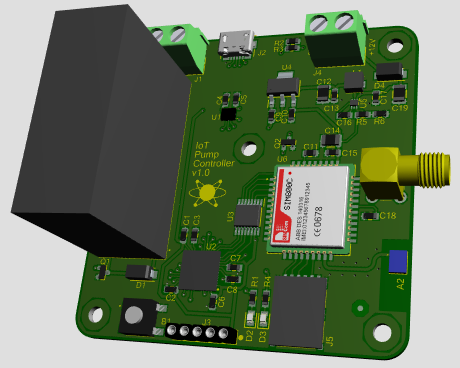
3D Visualisation of IoT Pump Controller Board
Circuit Description
The following is a block diagram showing the behaviour and interaction of the circuit components.
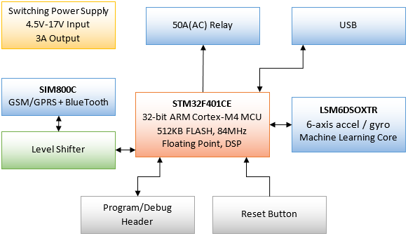
Block diagram of the IoT Pump Controller Design
We’ll cover the basics of the design construction as we progress through the tutorial but in order to keep the focus on the practical aspects of using the software, design decisions and theory will not be discussed in this document.
Advanced PCB Layout Features
We will be using a 4-layer PCB, with the following stackup:
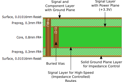
Layer Stackup
- The PCB will have components on the top side only. The top layer will contain component pads, signal traces, and a ground plane.
- Inner layer 1 will contain signal traces, and a power plane (+3.3V).
- "High-speed" (impedance controlled) traces will be routed on inner layer 2, referenced to the bottom layer which is a solid ground plane ("return path").
The following features will be implemented:
Track-length matching on the USB, SPI and ICSP lines. Whilst track-length matching on the SPI and ICSP lines is not really required, these provide a good opportunity to demonstrate the track-length matching feature without going into an overly complex design (such as one implementing DDR) for the purposes of a quick and concise tutorial.
- Differential pair routing and phase matching on the USB lines.
- Via shielding along the curved trace between the wireless module and the BlueTooth antenna.
- Keepout zone on the power planes around the BlueTooth antenna.
- Design-rule rooms allowing tighter routing and track-necking around fine-pitch components such as the microcontroller.