LIBRARY PARTS
Introduction
The Proteus Design Suite comes with a significant installed base of schematic components, almost all of which are already packaged with the correct PCB footprint. However, with the number of new parts entering the market every day and the vast choice available to engineers it is inevitable that users will have to either import library parts into Proteus or create library parts inside Proteus.
Importing Library Parts
Importing Library Parts is by far the preferred option. It is both much faster to do, is far less error prone and you can import both the schematic part and the layout footprint at the same time. Proteus supports two ways to import parts:
- Integrated Web Search and Import (Requires a valid USC)
- Manual Library Part Import Dialogue.
Short tutorial videos on working with both methods can be found on our Youtube Channel
Web Search Import
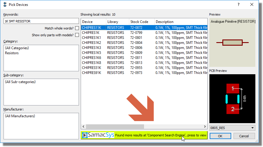
The integrated web search import works directly from the library picker dialogue. You simply type the part name you want and, after searching the installed libraries, you can search a database of over 15 million parts from our partner Samacsys. Just click on the yellow bar! This service requires a free account to be registered with Samacys and a valid USC to import the parts.
Library Part Import Dialogue
This method enables you to manually import via the Import Part command on the Library menu in either the schematic of the layout editors. This import will work with all major vendor files such as those generated by Ultra-Librarian, Samacys, SnapEDA and PCB Library Expert as well as through common supplier portals such as Digikey or RS Components. It does not require a valid maintenance contract to work but does involve slightly more effort.
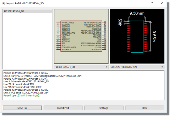
The Import Part dialogue with a part loaded.
Technically, the import works with PADS Library V9.x files, meaning that the import will work with any supplier who can generate a fileset in this format.
To import a library part using the library picker
Web search import works as follows:
1) Launch the library picker in the schematic module (also 'P' on the keyboard).
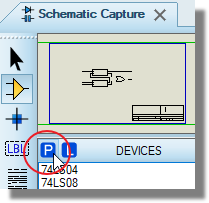
2) Search for a part. If matches exist in the installed libraries they will be shown and you can click to open web search results from the bar at the bottom of the picker. If there are no matches from the installed libraries you will go directly to web search results.
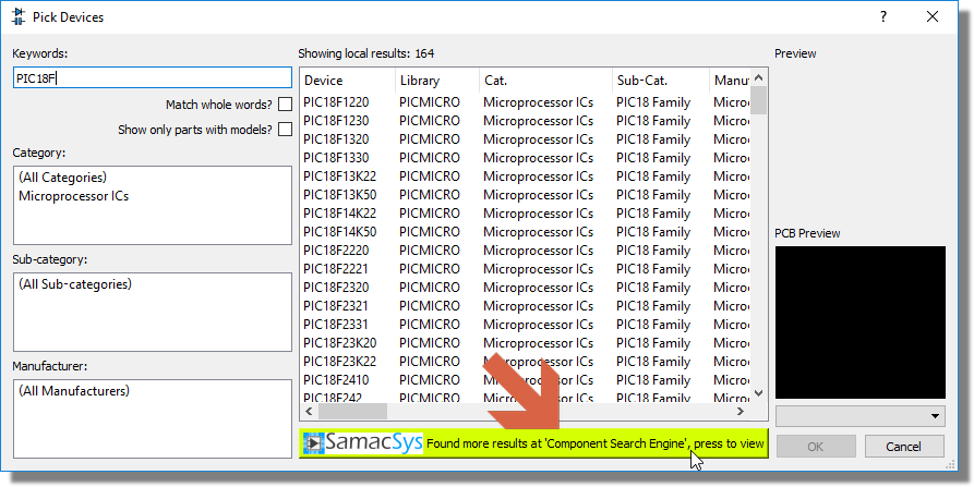
3) Results in normal font are available for import. Results in disabled text can be requested (at no charge) from the build service form.
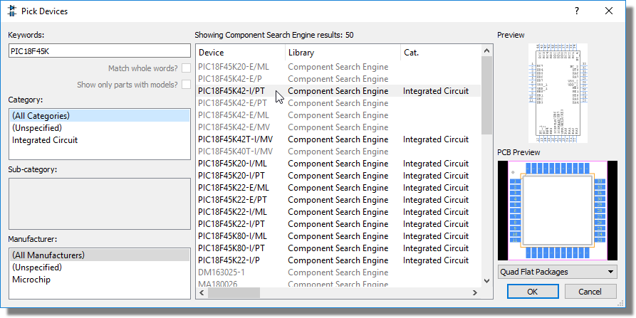
4) Double click to import. The first time you do this you will need to supply credentials or create a free account.

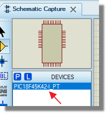
5) When you double click to import, both the schematic part and the associated PCB footprint will be brought into your user libraries and also picked into the current project. In most cases, the 3D STEP file for the footprint will also be imported.
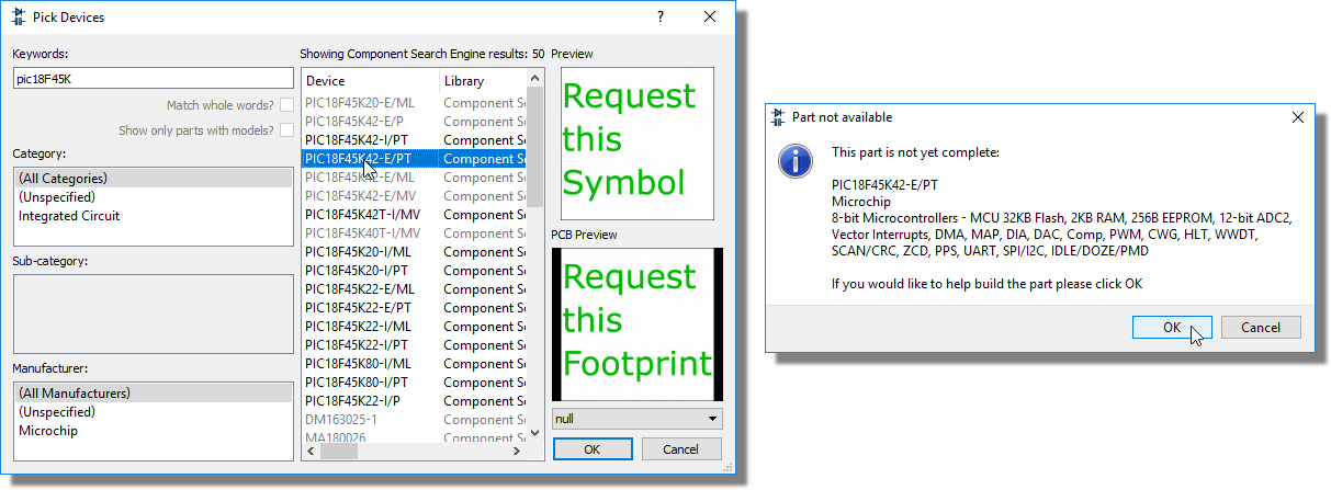
If you need to request a part to be made you can do so directly from the pick dialogue by double clicking on one of the disabled entries in the web search. The service is free of charge and average turnaround is 24-48 hours.
To import a library part using the dialogue
1) Download the part you want onto your computer. This will almost always be in a zip file.
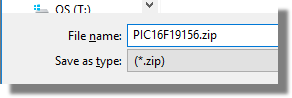
2) If the part doesn't come from a vendor source that we directly support (see here) then you'll need to extract all the files from the zip into a folder of your choice.
3) From the Library Menu in Proteus select the Import Part command
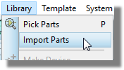
4) Click on Select File and use the file selector on the right hand side to select either generic PADS Library V9 files or the vendor of your choice.
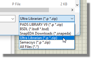
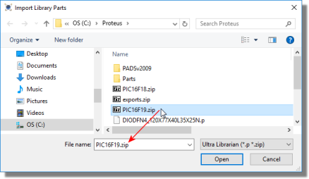
5) Choose the appropriate file to load. This will normally be a zip file if the vendor is selectable in the file selector or a .p file if you've had to extract the parts into a folder.
6) Review the parse log and the previews to make sure everything looks good. Use configuration settings if need be to fix problems.
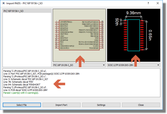
7) Use Import Part and follow the wizards to bring first the footprint and then the component into Proteus. This will both put the parts into your libraries and deposit them in the parts bin of the current project ready for placement. You should have an end parsed result that looks like the following:
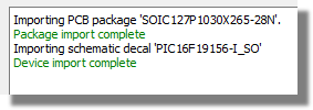
What you are actually doing at this last stage is running the Make Package tool to create the footprint and then running the Make Device tool to make the schematic component. The areas where input may be required from you are in the library choice and the description and categorization of the part.
For most complex devices, you can also find a BSDL script from the manufacturer. This is schematic part only but can be imported via the same import part command (select BSDL in stage 4 above).
Creating New Devices
If all else fails you can create parts yourself entirely inside Proteus. Alternatively, you may wish to permanently adjust the properties or footprints of an existing component. This section of the documentation starts from the basics of creating a new device and covers the entire process through to storing the new part in the library.
While the following topics are a detailed explanation of how to create component parts in Proteus, in practise this should almost never be necessary. In addition to the many installed libraries Proteus includes a web search with access to 15 million library parts and also the universal part importer provides support for almost all third party part vendors (Ultra-Librarian, Samacsys, SnapEDA, etc.). If the part doesn't exist in Proteus itself the next step is to search for and then import it directly from a third party vendor. This is discussed in some detail in the importer help file and shown on our Youtube Channel.
Graphics and Pins
For our example part lets assume that we want to create a Microchip MCP23008 I2C expander. The first thing we need to do is to create a graphical representation of the part on the schematic. When we are finished it should look something like the following:
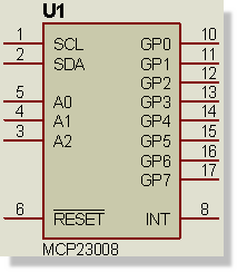
The MCP23008 Completed
Let’s begin by placing the component body as follows:
- Select the 2D Graphics Square icon and make sure the component style is selected in the Object Selector.
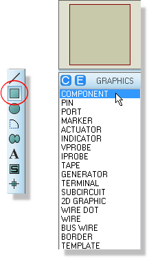
- Left click once on an empty area of the schematic to begin placement.
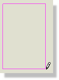
- Move the mouse until the rectangle is around the size of the part that you want. It’s better to make this slightly larger than might be required as we can easily resize it later.
- Left click again to complete placement of the graphic.
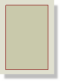
Proteus supports a powerful graphics style system of local and global styles and the ability of local styles to follow or track global styles that allows you to easily and flexibly customize the appearance of your schematic. See the section Graphics and Text Styles in the online reference manual for a complete explanation of how styles work and how they are used.
The next job is to place the component pins.
Select Component pin mode and make sure that you have the default pin
type selected in the Object Selector.
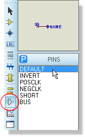
- Left click the mouse on the schematic to begin
placement. The small cross at the end of the pin indicates the side
of the pin that will be wired to so it is important that this is outward
facing.
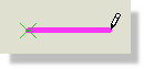
- Move the mouse so that the other end of the pin
touches the edge of the component graphic and left click again to
place
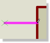
- A new pin is automatically primed for placement
so simply move the mouse down slightly and left click to place again.
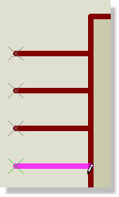
- Repeat the process down the left hand side of the component graphic using the completed screenshot as a reference. Right click to finish placement.
- Click on the X-Mirror icon to point the pin in the opposite direction ready for placement down the right hand side.
- Repeat as of stage 3 to place the pins down the right hand side of the component.
- Right click the mouse when you are finished to exit pin placement mode.
The Plus (+) and Minus (-) keys can also rotate the pin during placement, but you will find that when adding pin numbers, they will be on the opposite side of the pins that you placed before rotation. In this case right click on the pin(s) affected and click the Y-Mirror option to correct the pin(s).
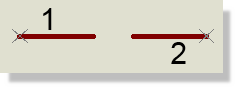
At this stage your component graphics should look something like the following:
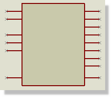
The body of the MCP23008
The actual positioning of the pins is of course somewhat aesthetic and you may prefer to have different groupings to those we have chosen.
Now that we’ve placed the pins we may need to adjust the size of the component body. If you need to adjust the size of the component body to better fit. To do this, click on the Selection Mode icon and simply left click on the edge of the component body, then left depress the mouse on one of the nodes, drag to the new size and release the mouse to commit.
This works much like any other graphics package. For example, if you right click along the bottom you can drag up and down and if you right click on an edge and you can drag diagonally. Make sure however, that you do not leave any of the pins ‘hanging’ (not touching) when you do this, else you will have to subsequently move the pins back onto the component edge.
If you want to make fine adjustments you may need to adjust the Snap level – these options are available from the View menu (defaulted to 0.1in) and are discussed in more detail in the reference manual.
Now that we have the basic shape of the part we need to add names to the pins. This can be done as follows:
- Right click on the pin at the top left of the component and select Edit Properties from the resulting context menu.
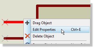
- Type in the name of the pin (SCL), the default pin number (1) and the electrical type (INPUT). You can use the other options to control visibility but for our purposes the defaults are fine.
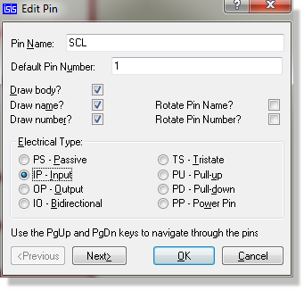
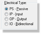
- Hit the Next button at the bottom to switch to the next pin in the list and repeat the process – the schematic will update to show which pin you are editing. If you are unfamiliar with this part and don’t therefore know the electrical type of the pin simply leave it as the default Passive type.
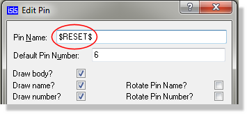
- When you get to the RESET pin you’ll need to add an overbar. Do this simply by adding a dollar (‘$’) prefix and suffix to the name.
- Hit the OK button when you are finished.
You may have noticed that there is a significant omission from the schematic part as we have drawn it so far, namely that there are no physical power pins on the device. Since we do not need to wire power nets explicitly we do not need a physical pin for the component. We need only ensure that the power pins are handled correctly with respect to the physical PCB footprint and we’ll discuss this in more detail in the next section. It is worth noting however, that while it is very common to have non-physical power pins in order to reduce clutter on the schematic, you may have a preference for everything to be explicitly wired. In this case you could simply add two extra pins and name them VDD and VSS respectively.
Our final task now is to make a device from the composite graphics and pins that we have placed. Start by drawing a tag box around the entire graphic (right depress the mouse and drag the selection box). Next, right click the mouse inside the selection box and select the Make Device option from the resulting context menu.
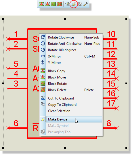
Make Device icon and the Context menu option
This presents us with the Make Device dialogue form, where we can customize the part. All fields throughout this wizard have detailed descriptions available when clicking on the help (?) icon on the top right of the window. However, the only items we need to deal with here are the Device Name and the Reference Prefix. The device name should be MCP23008 and the reference prefix should be ‘U’.
The reference prefix serves to categorize parts for Bill of Materials Output and is also used in annotation. These are fairly standard across the industry with ‘R’ denoting resistors, ‘C’ for capacitors, ‘U’ for IC’s and so on.
Use the Next button at the bottom of the dialogue to move onto the next screen.
Adding Footprints
In a previous section of the documentation we saw how to quickly add a footprint to a schematic part. This is useful for small passives and simple parts but, when we are creating a device we need to follow a more complete procedure. This ensures not only that we have a correct mapping between the pins on the component and the pads on the footprint but also allows us to better handle power pins.
From the screen on the Make Device dialogue form click on the Add/Edit button to launch the Visual Packaging Tool. The first thing we need to do is to find the footprint we want to use so click on the Add button at the top of the dialogue form.
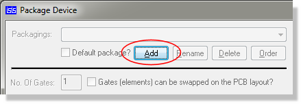
The 'Add' button in the Packaging Tool
This brings up the package browser dialogue which we covered earlier in the documentation. Assuming that we want the surface mount package, type SO18 in the Keywords field and then double click on the part in the results list to select it.
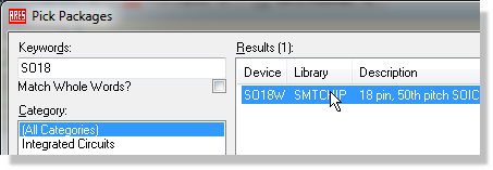
Selecting the SO18W from the package library
The Visual Packaging Tool will now look something like the following screenshot.
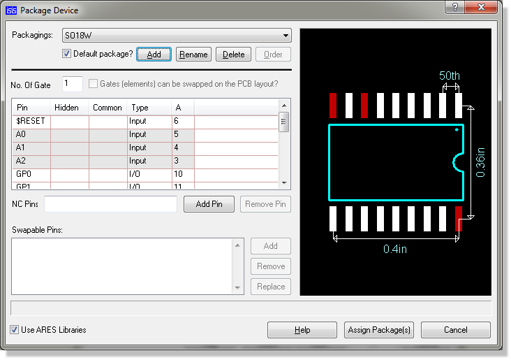
There are several points of note here. Firstly, the pads in the preview which are white are deemed to be mapped onto component pins. This has happened as we have correctly specified the default pin numbers when we edited the pins earlier on (pad name maps onto pin number when present). If we had chosen to leave the pin number fields blank we would have to map all of the pins in this dialogue form.
Secondly, we can see that there are three pads (7, 9 and 18) which are not mapped onto component pins. Normally we would have the datasheet beside us to get the footprint mappings but in this case pin 7 is an NC pin, pin 9 is the VSS pin and pin 18 is the VDD pin.
The NC pin is easily handled – simply type 7 in the field for NC Pins. Notice that the preview on the right hand side will update to show that this pad is now considered dealt with.
We now need to add two ‘virtual’ pins for the power pins. These are pins which don’t need to be on the schematic (their connection is made implicitly according to their name) as they will add unnecessary clutter, but do need to be mapped onto pads in the footprint.
If you want to have all pins visible on the schematic (e.g. for auditing purposes) you can certainly do so. You would add another three pins to the device, connect one of them to an NC terminal (to put on the NC net) and connect the other two to power terminals with the correct names. If you are in any doubt regarding power nets and connections please see the section earlier in the document on powering the circuit or consult the reference manual.
Click on the Add Pin button underneath the grid, type VSS to name the pin and then repeat the process for the VDD pin. Remember that connections to these virtual pins are made according to their name so make sure that you name them correctly.
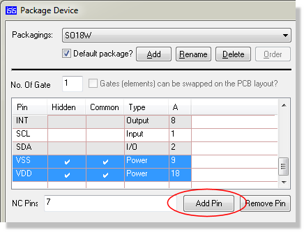
Adding a virtual pin
Having created the pins we assign them to pads on the footprint as follows:
- Click in the column at the far right of the VSS pin.
- Click on the corresponding pad on the footprint (pad 9).
- The cursor will move down to the next pin (VDD) so all we need to do is click on pad 18 on the preview.
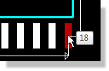
Clicking on pads will assign the pin
We should see that all the pads on the footprint are now highlighted, indicated that the part is fully packaged. Simply hit the ‘Assign Package’ button at the bottom of the Visual Packaging Tool to commit and return to the Make Device dialogue form.
It is possible (and extremely useful) to have more than one packaging for a given component. We could, for example, follow the exact same procedure to add a DIL18 footprint to the component. Where more than one packaging exists you can specify the one which will be used by default by checking the default box underneath the package name in the Visual Packaging Tool.
Click the next button at the bottom of the dialogue form to move onto the Property definitions section.
See Also:
Packaging Tool (Reference Manual)
Adding Properties
This screen allows us to add component properties to the device. We looked at doing this on a particular instance of a device (the part on the schematic) earlier in the documentation; the difference is that properties entered here will be stored in the master library part and therefore available every time we use the part in a design.
We can see that the PACKAGE property is already defined – this was what we configured visually on the previous screen
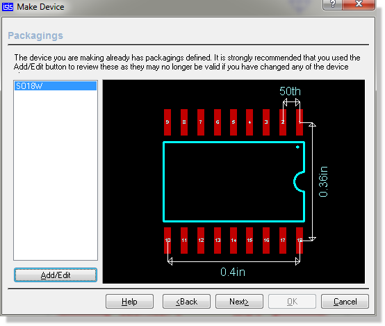
Package preview on the Make Device form
Let’s assume we want to add a property for RoHS compliance.
- Start by clicking on the New button at the bottom left and then clicking on Blank Item.
- On the right hand side fill out the name as ‘ROHS’ and the description as ‘RoHS Compliant’
- The next field is the data type which in our case is a simple Boolean (Yes/No) – select this from the drop down list.
- Change the Default value to be Yes and leave the visibility defaults as they are.
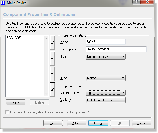
If you want to add more properties (e.g. MoQ, Price, Code, Supplier, etc.) simply repeat the process above. Alternatively, the Bill of Materials provides a convenient way to apply data to schematics as discussed earlier in the tutorial. Finally, for complete control or if you are doing this on a large scale, we recommend you read up on ASCII Data Import in the reference manual.
Click the next button at the bottom of the dialogue when you are finished to move on to the next screen.
Attaching a Datasheet
This screen allows us to attach a datasheet to the part we are creating. To do this we would need to enter the filename for the datasheet and then configure the path as required. As we don’t have a datasheet handy we’ll ignore this step but the following screenshot shows an example of how we would set it up.
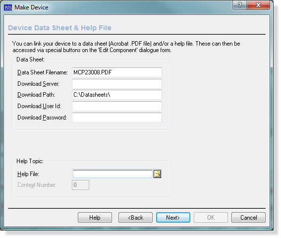
Adding a datasheet to the component
The main advantage of working through this step is to have the datasheet handy when you place the part. If present, you can simply edit the component and click on the Data button at the right hand side.
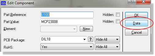
The Data button will launch the assigned Datasheet
For convenience, we have configured many of our library parts with datasheets which you can download from our web server via this button.
Indexing and Library Selection
The final screen allows us to categorize our part and choose which library we will place it in. As we have seen earlier in the tutorial the part description and the categories are used as filters when finding and selecting parts from the library so it is worth giving some thought to your description. An example of what you might enter is shown in the following screenshot.
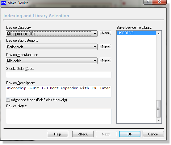
Final section where you save the component to a library
When you are finished simply click the OK button. You will be prompted to replace all instances of the device on the schematic – this allows you to update the current design if you are modifying a part which already exists on the schematic.
Finally, if you now select the part from the Object Selector and edit it’s properties you should see something like the following screenshot.
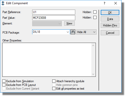
Edit Component for the MCP23008
It is also possible to create multi-element parts in Proteus. While beyond the scope of this tutorial these are covered in the reference manual.
See Also: