PCB LAYOUT
Preparing for PCB Layout
Now that we have completed the circuit we need to give some thought to PCB Layout and the information that we are going to provide from the schematic. Information is transferred from the schematic to the PCB layout via a "netlist". The netlist, in its most basic form, essentially consists of a set of footprint names (physical packages associated with schematic components - a resistor can come in various different shape and size "packages" for example) and connections (wiring on the schematic); it can however also contain additional information, such as wiring classes (e.g. POWER and SIGNAL) which can help make things easier for us later on.
If you do not have a completed schematic at this point or wish to work with the pre-supplied schematic you can load it via the Open Samples command on the Proteus home page. The file name is IoT_Pump-Schematic.pdsprj
Packaging Considerations
Each component on the schematic should be associated with a footprint in the PCB layout editor. Fortunately, the Proteus system provides a large set of pre-packaged components where one or more PCB Package options are already associated with the component, and most of the components on our design are already correctly packaged. We will want to change the packages of the generic RES and CAP components which we have used however.
To view the package associated with a component:
As previously covered in this tutorial, a number of options are available for changing component properties (some better suited to changing the properties of a single component, and some better suited to changing the properties of multiple components at once). To start, let's change the package of a single component. Find C1 (it should be on the "Microcontroller & IMU" schematic sheet) and edit it's component properties (right-click on the component, Edit Properties).
We could have chosen to only pick specific components from the library, which already had the correct package associated with them. As we have used generic parts however, this will afford us an opportunity to demonstrate changing a component's PCB package.
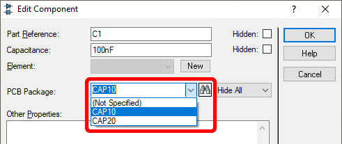
PCB Package Options
The generic CAP component has two packages associated with it by default (both of which are "through-hole").
You can also see what the default footprint is for a component at the time you pick it from the libraries. At the bottom of the Pick Devices dialogue form a preview of the footprint is shown for the currently selected component.
To change the package on a single component:
In our design we would like to use an 0805 SMD package, so click the search binoculars to launch the "Pick Packages" dialogue.
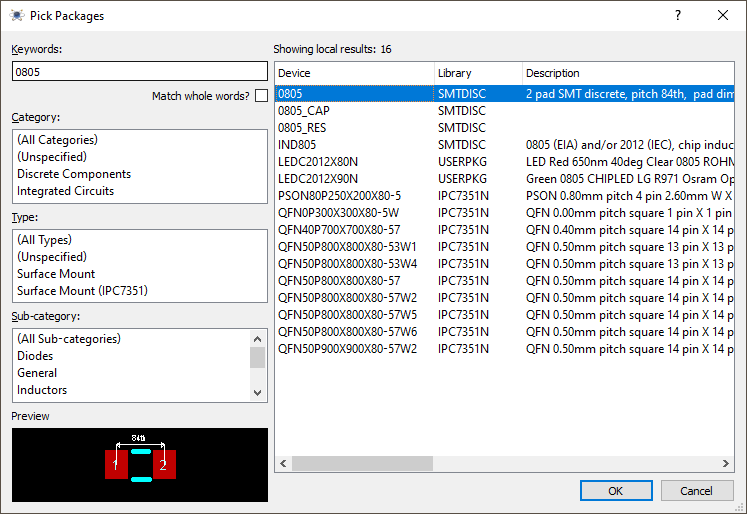
Pick Packages Dialogue
Type "0805" under Keywords, and a few options should be found. A preview of each package is displayed at the bottom-left of the window when the package is selected. Select the "0805" package and click "OK".

0805 Package Selected
The Category, Type and Sub-category filters can also be used to filter the search results.
The C1 part is now associated with an 0805 package. There are a couple of points to note here:
- If we knew the name of the package beforehand, then we could simply have typed it in ("0805") rather than using the Pick Packages Dialogue.
- Assigning a package in this way works because the Schematic Part and the PCB Package have the same number of pins with the same names. Where this is not exactly the case, the "Visual Packaging Tool" can be used to properly associate a PCB Package with a Schematic Part.
See Also:
Changing the package of each capacitor on the design one-by-one will be tedious however, so we will use the Design Explorer to do this more efficiently.
To change a package on all components of a particular type:
If we want to make a wholesale change to parts already placed then we can do so from the Design Explorer. First, open the Design Explorer via the icon on the main toolbar, and then switch to the search tab:
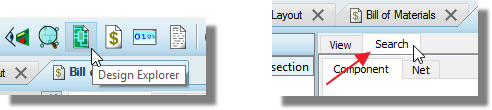
Following on from our example above, let's set category to be Capacitors, Value to be 100nF, and then hit search.
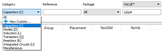
You should now see a filtered list of all the 100nF capacitors on the schematic in a grid view.
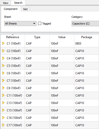
To change the package, simply type in the field at the top and then, much like Excel, drag the value down the other entries in the column.
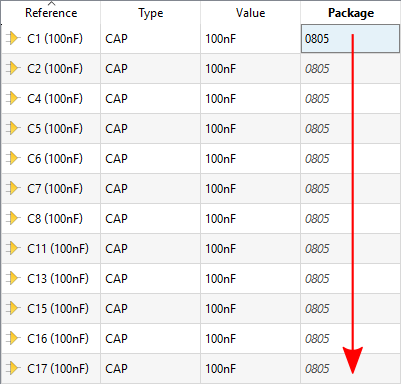
Some caution is required with bulk editing like this because the software will accept your input without verification. It is however, extremely handy for changing passive footprints en-masse.
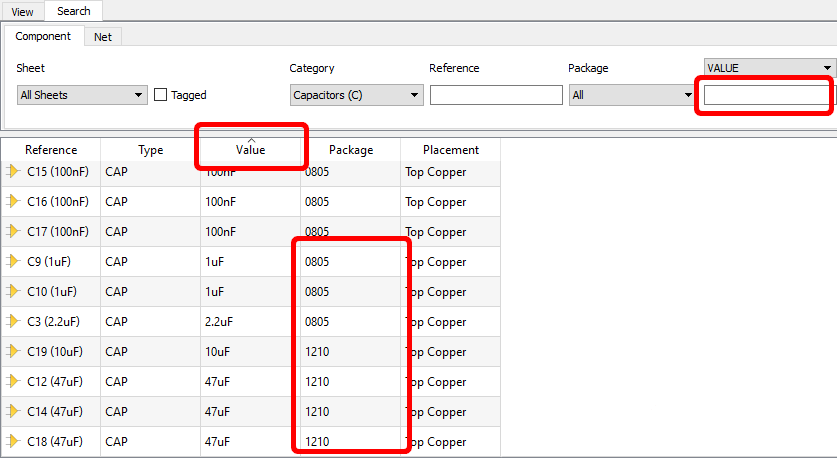
Let's assign packages to the remaining capacitors next. Search again within the capacitors category, but this time do not specify a value (leave the value field blank). Once the search results have been displayed, click the "Value" column header in order to sort the capacitors by value. Assign 0805 packages to the 1uF and 2.2uF capacitors, and 1210 packages to the 10uF and 47uF capacitors.
Next, let's change all the resistor packages to 0805. We could do this using the Design Explorer, but we will use the "Search & Tag" and "Property Assignment Tool" dialogues instead, in order to demonstrate their use. On the Schematic Capture tab, open the Search & Tag tool (binoculars icon).
We want to search for all components with a reference ("REF") beginning with "R".
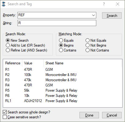
Our search turned up the relay ("RL1") as well, so we need to trim this from the list; change the search mode to refine the list, change the matching mode to "Not Begins", and search again for "RL".
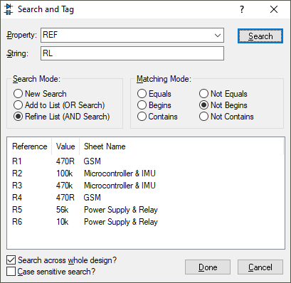
Click "Done" and all the components from the search list (R1-R6) will be tagged on the schematic. Next, start the Property Assignment Tool (wrench icon next to the binoculars icon).
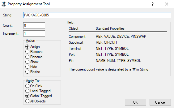
We want to assign a package of 0805 to all the globally tagged objects, so enter "PACKAGE=0805" in the String field and click OK; all the resistors which we tagged with the Search & Tag tool are now assigned an 0805 package. The Search & Tag tool combined with the Property Assignment Tool provide a flexible and powerful combination for bulk property editing.
Connectivity Considerations
When we transfer our schematic to the PCB Layout software (netlist) all of the wires and connections are grouped into nets and passed through. The schematic capture module actually does quite a lot of work for us behind the scenes at this point, automatically generating numerical names for the nets and also assigning the net to a default ‘net class’.
Net names are assigned on the schemaitc according to the following rules:
- A group of connections which include a named terminal will be assigned a net name according to the name of the terminal.
- A group of connections which include an unnamed ground terminal will be assigned to the GND net.
- A group of connections which include an unnamed power terminal will be assigned to the VCC net.
- Any other group of connections is given an auto-generated numerical name.
What this means in practice is that all the work is done for us here; there is no real need for us to get involved in naming groups of connections. It is important however, that we understand the rules for unnamed ground and power terminals. If in any doubt, you should always name your terminals explicitly.
If a net does not have a name from a terminal then you can, if you wish, explicitly name a net by placing a wire label with syntax (NET=NAME). This is useful if you wish to place a power plane on the net in the PCB Layout and otherwise helps to distinguish the net from other nets with auto-generated names.
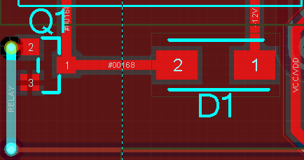
Net names displayed on the PCB layout
A ‘net class’ is simply a group of nets which will have common properties in the PCB Layout. Specifically, all connections in a net class will be assigned a default trace width and will obey a single set of rules with regard to clearances and design rules. Again, Proteus will do a considerable amount of work for us and will assign net classes as follows:
- Any net with a power or ground terminal is assigned to the POWER net class.
- Any net with a bus is assigned to the BUS net class.
- Any other net is assigned to the SIGNAL net class.
This gives us quite a bit of flexibility during PCB layout as we can define different trace widths, via styles, clearances and so on for each net class. Sometimes, however, we will need a particular set of conditions for particular connections. We are therefore allowed to create our own net classes on the schematic and these will then be passed through to the PCB Layout software, allowing us to define routing and clearance properties specifically for those connections.
In our design, we will want to assign a net class to the Power Relay tracks, as these will carry high voltage and high current and so we will want to increase the track width and clearance rules.
To specify a new net class
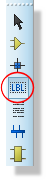
- Select the Wire Label Icon.
- Left click the mouse on the wire we wish to assign the net class to. In our case the net classes should be assigned to the wires between the relay and the terminal block.
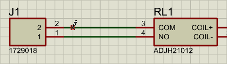
- Left click the mouse over the wire to launch the wire label dialogue form. Then simply type in ‘CLASS=RELAY_SW’ to assign the net class.

With both wire labels added it should look like the below.
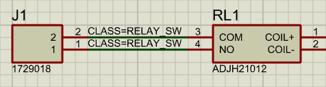
Nets connected to power terminals are automatically assigned to the POWER class. Sometimes intermediary wires, such as those between fuses and/or polarity protection diodes, are not directly connected to a power terminal however and so manually need to be assigned to the POWER class.
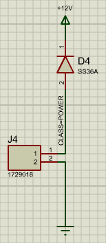
In our case this is needed:
- Between the power input and polarity protection diode.
- Between the relay COIL- and 2N7002 transistor.
- Between the DC-DC converter SW and the 3.3uH inductor.
If you have completed drawing the schematic follow this procedure now to add the net classes; this will already be in place if you have loaded our pre-supplied schematic. If you work through the PCB layout tutorial, you'll see how to configure routing styles and design rules for the net class.
Before moving on, if you have decided to complete the schematic layout and net classes yourself, then there is one more net class label that must be added. This is the "CLASS=50_OHM" label on the GSM schematic sheet. This label needs to be applied to the wire connection between the sim800c (pin 32) and SMA connector ("73100-0115" - pin 1). Additionally, the same label must be applied between the sim800c (pin 20) and the Bluetooth RF antenna ("A10192" - pin 1). This label will allow us to ensure that the associated trace conforms to a 50Ω impedance characteristic.
See Also:
Routing Classes (Reference Manual)
Defining a Net Class (Reference Manual)
Groups
When it comes time for PCB Layout, there are usually physical constraints as to where components should be placed on the board. Some components may need to be placed in a specific area of the board (such as connectors), and some components typically need to be placed physically close by to other components (the decoupling capacitors and crystal oscillators of a microcontroller, for example, should typically be placed physically close by to the microcontroller). When using the component auto-placer, we can help it with both of the aforementioned tasks by specifying "placement rooms", which are areas of the board within which certain specific components should be placed. We will tackle the drawing of the placement rooms in the PCB Tutorial, however in preparation for this we need to assign some components to groups which will then be associated with the placement rooms.
Let's start by specifying a group for the IMU (LSM6DSOXTR) and its two 100nF decoupling capacitors. What we need to accomplish here is to add a "GROUP" property to each of the components in the group, set to a common value (in this case, "GROUP=LSM6DSOX"). As previously discussed there are a variety of options for assigning properties to components in Proteus, however the Design Explorer is probably the best suited option for this task. Start by tagging (selecting) all of the components to be placed in the group (as we have laid out the schematic in sections already, this should be easy):
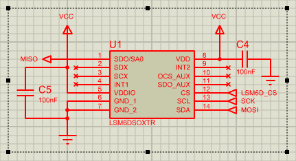
Next, open Design Explorer and search for all tagged components (no other filters - clear the category and value filters if they were set previously).
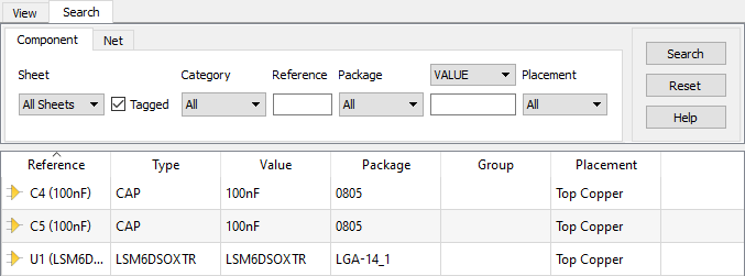
Search for all tagged components
Now, simply enter a group name ("LSM6DSOX") in the Group column for each component (as we saw previously when assigning packages, values can be dragged into other cells "Excel style" - a dropdown is also available on each Group cell, containing the names of all existing groups).
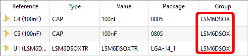
LSM6DSOX Group
The following groups should be created for this design:
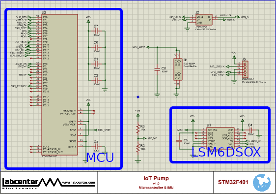
MCU and LSM6DSOX groups
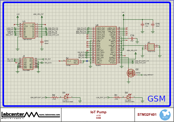
GSM group (everything on GSM sheet)
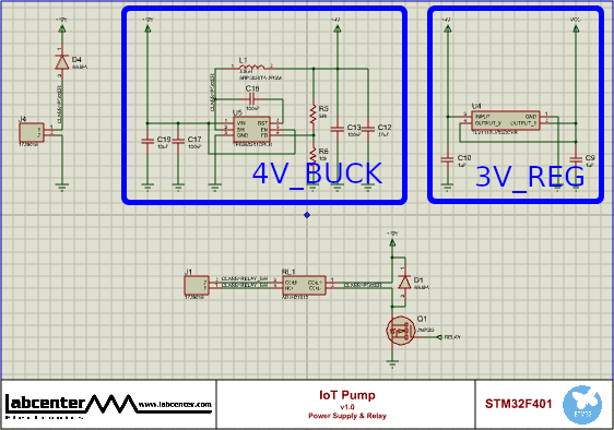
Power Supply groups
Differential Pairs
Differential signalling is a method of wired communication which has good immunity to electromagnetic interference. On a PCB, traces which are used for differential signalling are called Differential Pairs.
If there are any differential pair routes in a design, then we need to let the PCB layout know about these by tagging them on the Schematic. Specifically, we need to:
- Add a "DIFFPAIRS" property to each component which we would like to route differential pairs for.
- Add a "PAIR" Wire Label to one of the wires in each differential pair.
In our design, the USB connection includes a differential pair (the "D+" and "D-" lines), so we need to set this up on the schematic. Specifically, we need to:
- Add a "DIFFPAIRS=PA12,PA11" property to the STM32 microcontroller.
- Add a "DIFFPAIRS=D+,D-" property to the microUSB connector.
- Add a "PAIR=USB" wire label to either the USB_D+ or USB_D- line.
The DIFFPAIRS property on the components should be set to the names of the relevant pins on the component (not the numbers). The PAIR Wire Label only needs to be placed on one of the differential pair wires, and can be given any sensible value you like (although it should be unique).
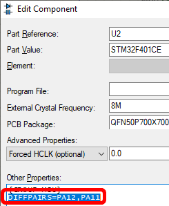
Differential pair setup on the STM32 microcontroller
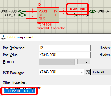
Differential pair setup around the microUSB connector
If you do not want the "DIFFPAIRS" property to be visible on the schematic, then place the property name and value within curly braces - i.e. {DIFFPAIRS=PA12,PA11} on the MCU and {DIFFPAIRS=D+,D-} on the microUSB connector.