DESIGN WALK
Introduction
It is often useful to follow a net through the various sheets of the schematic. The design walk feature provides a convenient way to do this using net tagging on the schematic sheets as a visual indicator.
The Design Explorer module by contrast provides a full data driven analysis of net contents and can also be viewed per sheet. See Design Explorer, Netlist View.
Tagging a Net on a Sheet
The design walk is started by specifying the net. This is done on the schematic by right clicking on a wire, terminal or pin of that net and selecting the 'Highlight Net on a Sheet' option from the context menu. Two sibling commands sit alongside it: 'Highlight Net on current Sheet' tags the net where you are without moving off the sheet, and 'Highlight Net on PCB Layout' tags the same net over in the layout.
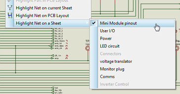
Highlight Net on a Sheet shows both which sheets contain the net and also the current sheet (with a tick).
All of the sheets on the current board are listed in order, with those not containing the net disabled. Sub-sheets are indented with leading hyphens, one per level of the hierarchy, so you can see where each sheet sits. The checkbox on the left hand side shows the current sheet. Left clicking on a sheet will tag it and navigate the schematic to that sheet.
The sheet list is built the first time you open the submenu, which requires the netlist to be compiled. On a large design there may be a short pause before the list appears.
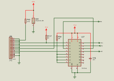
3.3V net tagged on a sheet.
You can also tag a net on a sheet from the Design Explorer module. First make sure you are in Netlist Mode and then right click on a net and select the Show Schematic Net option from the context menu.

Selecting a net on a sheet from inside the Design Explorer.
Walking the Design
Once you have the net tagged on one sheet you can cycle the sheets with the PGUP and PGDN keys. These are the shortcuts for the Design menu commands Goto Previous Sheet and Goto Next Sheet, so they work whether or not a net is tagged. Navigation on a multi-sheet hierarchical design is down then across.

Use the PGUP and PGDN keys to switch through the sheets.
Alternatively, if you want more control just right click on the wire again and select your next destination sheet from the list.
Following a Signal
Let's assume you want to follow a signal on the schematic. In our case, we'll choose an RS232 line. It's very likely that this will be on only one or two of the sheets. The best solution is therefore to use the context menu twice since it shows you on which sheets the signal is present. So:
- Right click and tag on current sheet.
- View.
- Right click and tag on next sheet signal is present.
- View.
- etc
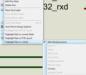
Use the Sheet states for faster navigation.
Checking Power
The other common use case will be to look at the IC's on the schematic and check that everything is powered. In this case the net will be a power net and is likely to be on most every sheet on the schematic. In this case cycling through the sheets with PGUP/PGDN after the initial tag is probably going to be easiest. So:
- Right click and tag on current sheet.
- View.
- PGDN.
- View.
PGDN
...
Needless to say this is only going to work well if you have visible power pins. If you use hidden power pins then they cannot be highlighted because they are hidden. You should use the Design Explorer's Netlist View in this situation.
Status Bar
The sheet name is shown on the status bar after you switch to it so you have some idea of where you are on the design hierarchy when cycling through sheets.

The status bar names the tagged net and the sheet you have arrived on.
It will also tell you if there is no net presence on the sheet. Assuming this is intentional, you can then just continue PGUP/PGDN cycling to the next sheet.

The status bar reports when the tagged net is not present on the sheet.