MULTI-SHEET DESIGNS
Multi-Sheet Designs and Connectivity
It is increasingly common in larger designs to split the schematic into multiple sheets. This serves both to reduce clutter on the schematic and also to organise the design into logical blocks. The Proteus schematic capture fully supports this methodology and we have arranged our tutorial design into two sheets in order to cover the relevant procedures. The work we have done so far has been to complete the first sheet (processor, sensors and memory circuitry), meaning we still need to cover the analog and power circuitry. We’ll do this on a separate sheet.
While beyond the scope of this tutorial it is worth mentioning that Project Clips provide a method for re-using logical blocks of design and layout. More detail is in the reference manual and a short tutorial movie is linked below.
Introduction to working with Project Clips
Also, note that what we are doing here is adding a second sheet at the same level as the first sheet. Proteus fully supports hierarchical designs where you use sub-circuits to contain logical blocks. This is discussed in detail in the reference manual.
See Also:
Multi Sheet Flat Designs (Reference Manual).
Sub-circuits (Reference Manual)
Project Clips (Reference Manual)
Practical Examples: Duplication of Design Hierarchies (Reference Manual)
Adding Sheets to a Design
To add a new sheet to the schematic we simply invoke the command from the Design menu as shown below.
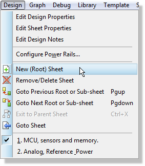
Creating a new sheet
Try this now to generate the second sheet.
Naming, Ordering and Navigating Sheets
Before we lay out the circuitry on this sheet we need to do a little housekeeping. While it’s not necessary it is often helpful to name the different sheets on the schematic and also to order them in some sensible fashion. We can do both of these things via the Edit Sheet Properties command on the Design Menu.
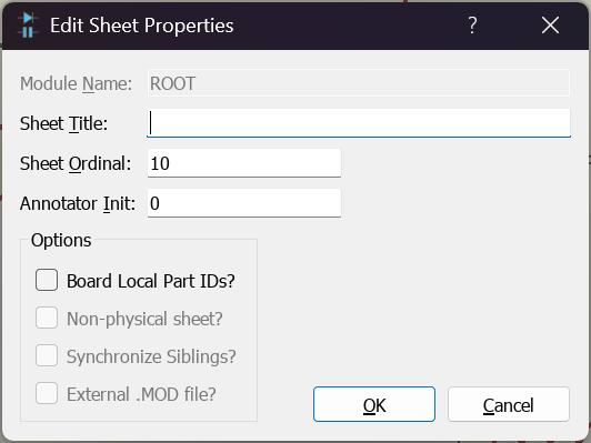
The Edit Sheet Properties dialogue form
The Sheet Title is what will be displayed and should therefore reflect the contents of the sheet. In our case let’s name it ‘Analog, Reference & Power’.
Sheets on the schematic are organised by Sheet Ordinal and by default these are 10, 20 and so on. A sheet with an Ordinal of 20 will therefore appear behind the first sheet (default Ordinal 10). If you prefer purely numeric nomenclature we can change the sheet name to be ‘2’, to better reflect it’s position in the design structure.
The default sheet names may seem inconsistent. This is because there is also a Master Sheet, present in all designs, which allows the application of a company logo, revision number, author and other schematic information. This is beyond the scope of this tutorial but more information can be found in the Templates chapter of the accompanying reference manual (Help Menu – Schematic Capture Help).
Sometimes, it is desirable to have a base annotation for a sheet; this means that the global annotator will increment from the value entered in this field. For example, if we set this to be 100 then the first resistor placed on the sheet would be annotated as R100. When left at it’s default value the global annotation will continue from it’s current position – this is fine for the purposes of the tutorial.
Setting initial annotation for sheets is useful as it can guide the Global Annotator when batch annotating. It can - if you choose - also then be honoured when annotating physically via the Automatic Annotator in the PCB Layout Module.
Before exiting, your dialogue form should now look something like the following:
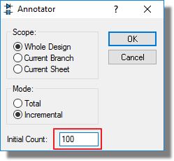
Global Annotator with the Initial count set.
For completeness we should also follow this process for the sheet we have just finished laying out. Before we can change the properties of a sheet we must first navigate to that sheet in the design and Proteus provides several ways to do this :
- From the Design Menu select Root Sheet 2 at the bottom of the menu,
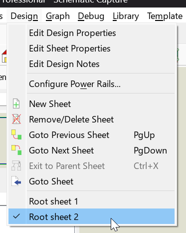
- From the Design Menu, select the Goto Sheet command, select the sheet and click OK to switch to that sheet.
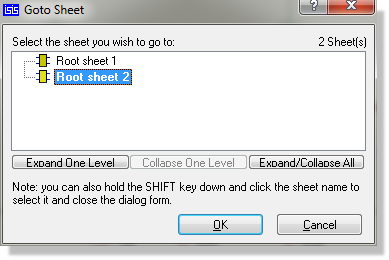
- Use the PGUP and PGDOWN keyboard shortcuts to navigate between sheets. These cycle up and down the sheets respectively, although for a two sheet design they will seem to have the same function!
The Design Explorer is also a powerful way to navigate the schematic – this is covered in the Design Verification section of the tutorial and in more depth in the reference manual.
Once you find yourself back on the sheet we have laid out simply repeat the process above, with a sheet title of ‘MCU, sensors and memory’ and a sheet name of ‘1’.
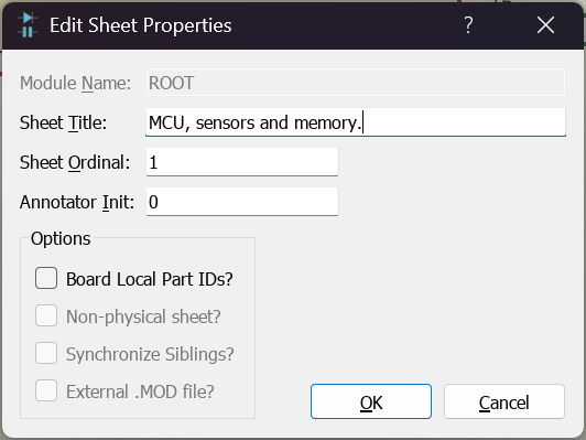
Sheet 1 properties
You should now see correctly organised and labelled sheets at the bottom of the Design Menu
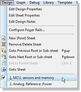
This is what you should see in the Design menu
Connectivity between Sheets
Now that we have taken care of the naming, let’s navigate back to our blank sheet and lay out the analog circuitry. The following screenshot shows the circuit we need to draw.
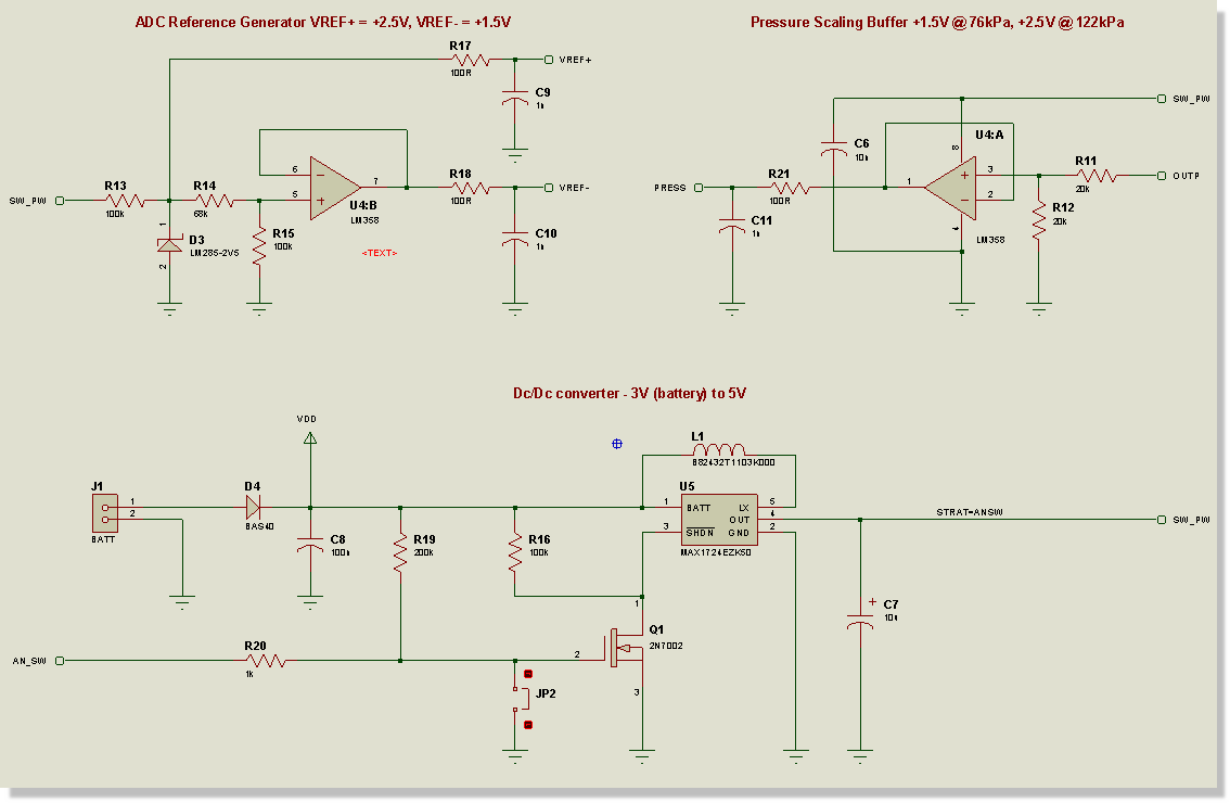
As we can see, there are three logical blocks of circuitry; a reference generator for the ADC module, an analog buffer for the pressure channel and a DC/DC converter to provide 5V from the 3V battery to the other two sections on each pressure sampling time.
If you feel that you need more practice then you can use all of the techniques we have covered so far to complete the schematic. Alternatively, if you are comfortable with the basics of schematic entry we will load a pre-supplied completed schematic in the next section. Regardless, there are a couple of points of note that are worth emphasising.
As each of the three blocks comes together, group it in the way we did on the first sheet: tag a box around it, right click and choose Group Objects. Groups are per object rather than per sheet, so the sheet you are on makes no difference, and we shall put these three to work shortly when we come to arrange the sheet properly.
Firstly, connectivity between sheets is achieved by having terminals with the same name on both sheets. From the screenshot above you can see the named terminals and, switching to the first sheet, the corresponding terminals with the same name. This technique allows signals to propagate not only across a sheet but also across sheets.
See Also:
Secondly, it is possible when placing wires to ‘guide’ the wire placement as you place the wire. This is achieved by left clicking the mouse as you change direction, placing an ‘anchor’ to help the follow-me algorithm place the wire the way you want. Typically, this is useful on more complex wire trails but we can look at a simple example for the purposes of illustration.
Consider the connection between the negative input of U4:B and resistor R18 as shown below.
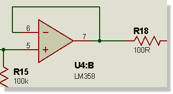
Negative input wire to R18
If we delete this wire (right click and select delete), we could replace the connection in the usual way and the follow-me algorithm would make a decent job of it. However, if we wanted to be more precise we could proceed as follows:
- Hover the mouse over the negative input such that it turns green and then left click to start wire placement.
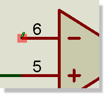
- Move the mouse along to the left and then left click the mouse once to place an ‘anchor’.
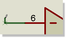
- Move the mouse up, left click to place an anchor, then right, left click to place an ‘anchor’ and finally down onto the wire between the op-amp output and resistor.
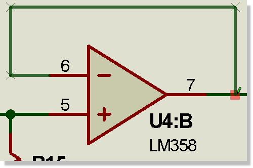
This technique constrains the follow-me algorithm and provides greater control during wire placement. If at any time during placement you change your mind and wish to remove an anchor simple right click the mouse once. Finally, if you want to completely disable the wire-auto-router and, for example, place a wire at 45 degrees, simply hold the CTRL button down on your keyboard during placement.
Gateswap
Now that we have a multi-element placed (LM358 dual op-amp) it's a good time to look at gate-swapping on the schematic. The reference for a multi-element part reflects both it's part reference (e.g. U4) and also it's gate element identifier (e.g. A) as shown below.
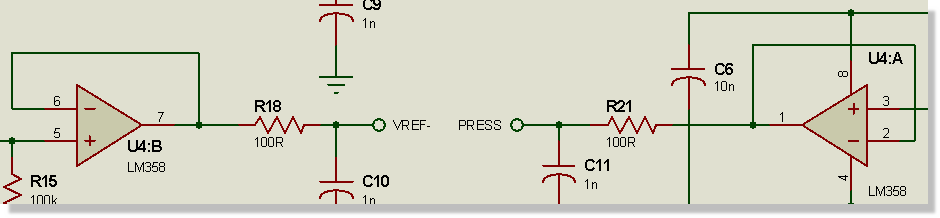
U4:A and U4:B
Start by editing one of the LM358 gates (right click - edit properties) to bring up the Edit component dialogue form.
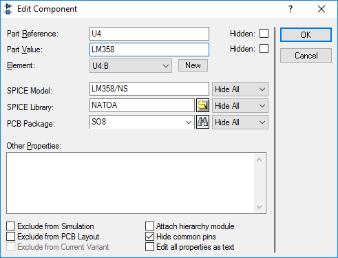
Edit Component Dialogue form for an Op-Amp
To swap the gates we are switching the element identifiers (A and B) on a single part (U4). The element field of the dialogue conveniently contains a combo box will all available gates so all we need do is change the element and hit OK to commit.
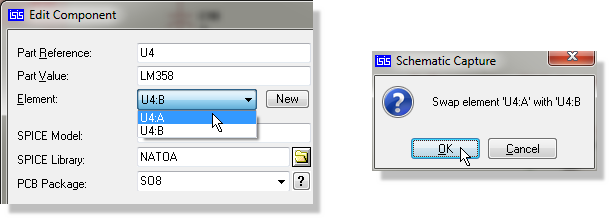
On schematic this switches the gates over according to the change specified in Edit component.
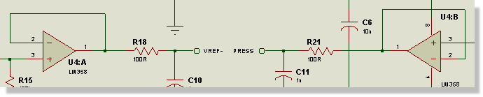
See Also:
Gateswap on Schematic (Reference Manual)
Arranging the Schematic
The drawing part of the tutorial is now complete. If you chose not to draw the second sheet yourself you can simply read through this section, since the pre-supplied project is already arranged in the way described here. Before we move on it is worth spending a few minutes on presentation, because a schematic is a document as much as it is a netlist and somebody, quite possibly you in six months' time, is going to have to read it.
The convention worth following is that signals flow left to right. Inputs and sources belong on the left of the sheet, processing in the middle and outputs on the right, with power at the top and ground at the bottom of each block. On our second sheet that means the DC/DC converter and the reference generator sit to the left of the analog buffer they feed. Nothing about the netlist changes when you do this, but the sheet becomes far quicker to follow.
This is where the groups we made earlier pay for themselves. Each block moves as a single object, so re-ordering the sheet is a handful of drags rather than a careful series of tagbox selections, and nothing inside a block can be left behind or knocked out of alignment on the way. Pick up any member of a block, drop it where you want the block to sit, and move on to the next one.
Once the blocks are where you want them, cast an eye over the wires and terminals between them. Wires attached to an object are re-routed automatically as it moves and the result will occasionally take a route you would not have chosen, so nudge any terminal or label that has ended up somewhere awkward and drag any wire segment that has taken the long way round.