PCB LAYOUT
Preparing for PCB Layout
The circuit is drawn and checked, so we can now give some thought to PCB Layout and the information that we are going to provide from the schematic. A netlist basically consists of a set of footprint names (packages associated with schematic components) and connections (wiring on the schematic), although we can make things easier for ourselves later on by providing additional information.
Packaging Considerations
Ideally, each component on the schematic should be associated with a footprint in the PCB editor. While you can do this at the point of placement in the layout editor best practise would be to sort this out in the schematic. Fortunately, the Proteus system provides a large set of pre-packaged components where this work is all done for us. As a case in point, almost every part we selected from the libraries for the data recorder arrived with a footprint already assigned; the only exception was the LED, and we dealt with that in the previous section when the Design Explorer flagged it as MISSING. The schematic therefore needs no further packaging work before we hand it over.
However, it is possible that you may want to change the footprint associated with a part (e.g. PTH to SMT). We’ll use the current schematic as a playground to explore how we can view and change packages to components.
To view the package associated with a component:
The footprint for a component is simply a property of the component on the schematic. We can therefore easily view the footprint by editing the component. Try this now by right clicking on one of the resistors on the schematic and selecting Edit Properties from the resulting context menu. You should see that there is a PCB Package property on the dialogue form and that the part is packaged with a standard 0805 footprint.
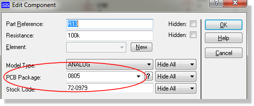
The new package appears in the Edit Component Dialogue form
You can also see what the default footprint is for a component at the time you select it from the libraries. At the bottom of the Pick Devices dialogue form a preview of the footprint is shown for the currently selected component.
For convenience, components in the schematic often have packagings for more than one footprint. For example, if you launch the Edit Component dialogue form for the dsPIC33 component you will see that you have the option of either an SO18W or a DIL18 footprint. In this case the designer can simply change the footprint if required via the Edit Component dialogue form.
To change a package on a component
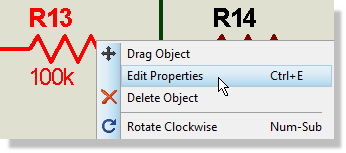
- Launch the Edit Component dialogue form by right clicking on the resistor and selecting Edit Properties from the resulting context menu.
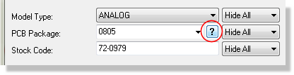
- Click on the question mark to the right of the package property to launch the footprint browser
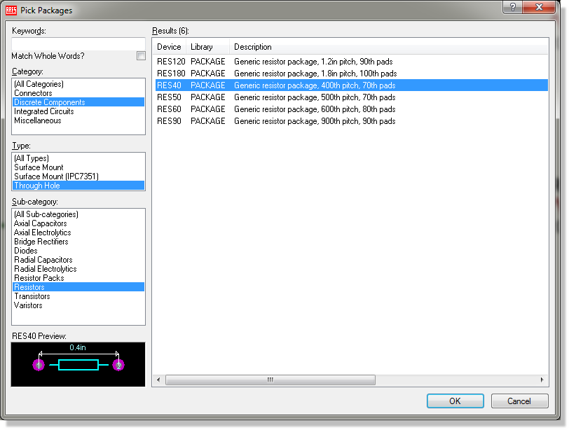
- Clear out the text from the keywords field and then use the filters on the left hand side to narrow down the selection. We will want to select the ‘Discrete Components’ category with type ‘Through Hole’ and Sub-Category ‘Resistors’. We can then select for example the ‘RES40’ footprint and click OK to commit.
- You should now see that the RES40 is listed as the PCB Package for the component in the schematic.
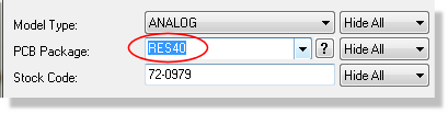
That was a demonstration rather than a design change, so set the PCB Package field back to 0805 before we go any further. A through hole footprint on a surface mount resistor would cause no end of confusion later in the layout editor.
To change a package on all components of a particular type
If we want to make a wholesale change to parts already placed we can do so from the Design Explorer, which we met in the previous section. Open it via the icon on the main toolbar and then switch to the search tab:
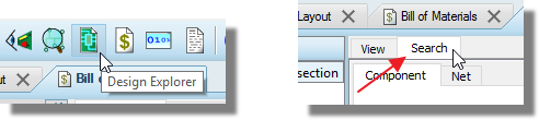
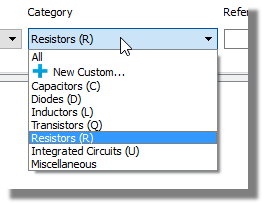
Following on from our example above, let's set category to be Resistor and hit search
You should now see a filtered list of all the resistors on the schematic in a grid view. We could filter further by entering a resistor value.
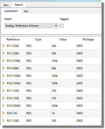
To change the package, simply type in the field at the top and then, much like Excel, drag the value down the other entries in the column.
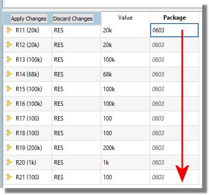
Hit Apply Changes to commit the change.
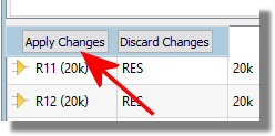
Some caution is required with bulk editing like this because the software will accept your input without verification. It is however, extremely handy for changing passive footprints en-masse.
See Also:
Connectivity Considerations
When we transfer our schematic to the PCB Layout software (netlist) all of the wires and connections are grouped into nets and passed through. The schematic capture module actually does quite a lot of work for us behind the scenes at this point, automatically generating numerical names for the nets and also assigning the net to a default ‘net class’.
Net names are assigned on the schematic according to the following rules:
- A group of connections which include a named terminal will be assigned a net name according to the name of the terminal.
- A group of connections which include an unnamed ground terminal will be assigned to the GND net.
- A group of connections which include an unnamed power terminal will be assigned to the VCC net.
- Any other group of connections is given an auto-generated numerical name.
What this means in practice is that all the work is done for us here; there is no real need for us to get involved in naming groups of connections. It is important however, that we understand the rules for unnamed ground and power terminals. If in any doubt, you should always name your terminals explicitly.
If a net does not have a name from a terminal you can if you wish explicitly name a net by placing a wire label with syntax (NET=NAME). This is useful if you wish to place a power plane on the net in ARES and otherwise helps to distinguish the net from other nets with auto-generated names.
A ‘net class’ is simply a group of nets which will have common properties in the PCB Layout. Specifically, all connections in a net class will have the same trace width and will obey a single set of rules with regard to clearances and design rules. Again, Proteus will do a considerable amount of work for us and will assign net classes as follows:
- Any net with a power or ground terminal is assigned to the POWER net class.
- Any net with a bus is assigned to the BUS net class.
- Any other net is assigned to the SIGNAL net class.
This gives us quite a bit of flexibility during PCB layout as we can define different trace widths, via styles, clearances and so on for each net class. Sometimes, however, we will need a particular set of conditions for particular connections. We are therefore allowed to create our own net classes on the schematic and these will then be passed through to the PCB Layout software, allowing us to define routing and clearance properties specifically for those connections.
Let’s take an example. On the tutorial schematic consider the output of the DC/DC converter on the Analog sheet of our design. This is the 5V switched power supply for the analog circuitry so we really want to lay this out with a track width smaller than that on the POWER net class but larger than on the SIGNAL net class. The procedure for specifying a new net class is very straightforward.
To specify a new net class
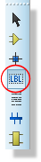
- Select the Wire Label Icon.
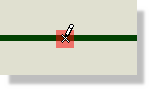
- Left click the mouse on a wire we wish to assign the net class to. Any wire on the net will do – in our case let’s place it between the output of the MAX1724 and the SW_PW terminal. You will see a small ‘x’ under the cursor when the mouse is over the wire.
- Left click the mouse over the wire to launch the wire label dialogue form. Then simply type in ‘CLASS=ANSW’ to assign the net class.
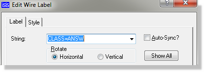
If you have completed drawing the schematic follow this procedure now to add the net class; this will already be in place if you have loaded our pre-supplied schematic. If you work through the PCB layout tutorial, you'll see how to configure routing styles and design rules for the net class.
See Also: