CROSS PROBING
Introduction
Cross probing is basically the ability to navigate to a component, a footprint or a set of connections from a different place. Design Explorer enables the following :
- Navigate to one or several schematic parts.
- Navigate to a sheet on the schematic.
- Navigate to a net on the schematic (highlight wires)
- Navigate to a net on the PCB (highlight tracks)
- Navigate to one or several PCB parts (if placed !)
Navigate to Schematic Parts
To navigate to a part while browsing:
- Right click on the part of interest and select
the Goto Schematic Part menu option from the resulting context menu.
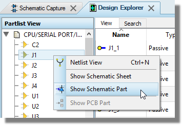
- The design explorer will minimise to the taskbar and the schematic will zoom in around the now highlighted part.
Note that you can navigate to a schematic part either by right clicking on a component or by right clicking on a pin, the latter providing a useful way to find a part while in netlist mode. You can also use the Schematic icon at the top of the Design Explorer as a shortcut when a component is selected.
You can also hold the CTRL button down and select multiple parts on the right hand pane and then use the same context menu to show on schematic. This will highlight all of the selected parts and take you to the first sheet.
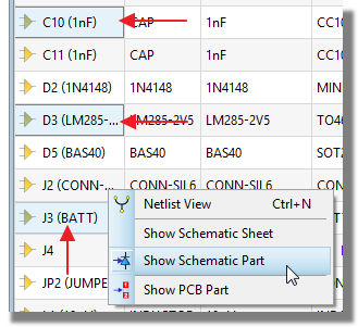
To navigate to a part when you know its reference:
- Launch the Design Explorer (Default shortcut key ALT+X)
- Launch the find dialogue from the top of the design explorer and type the reference into the edit field.
- Follow the steps outlined in the case above to navigate to the part.
You can also do this with the Search and Tag command inside the Schematic Module (keyboard shortcut T)
Navigate to Schematic Net
This action will highlight the specified net, tagging all wires on that net in the current sheet.
To tag and show a schematic net:
- Make sure you are in Netlist Mode or are at the level where you have a pin display on the right hand pane.
- Right click, either on a pin if at that level,
or on a net and select the Goto Schematic Net option from the resulting
context menu.
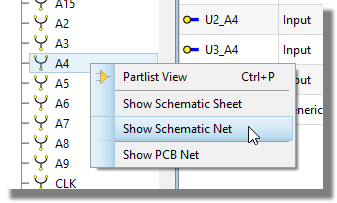
- The design explorer will minimise to the taskbar and all wires on the specified net will be tagged on the current sheet.
See the section on examples below for a walkthrough on performing more practical tasks with the design explorer.
Navigate to Schematic Sheet.
This action allows you to navigate between sheets on a complex multi-sheet design.
To navigate to a particular sheet on a schematic:
- Launch the Design Explorer.
- Ensure that you are in Partslist View.

- Right click on the sheet you want to navigate to
and select the Show Schematic Sheet option from the resulting context
menu. If you want to go to a child sheet you must first click on the
parent sheet to expand it. For deeply nested sheets you may find it
quicker to use the find tool.
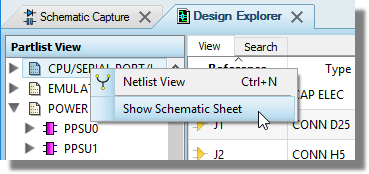
- The design explorer will minimise to the taskbar and the schematic will display the designated sheet.
Cross Probing to the PCB
You can action a cross-probe to the PCB in one of three ways:
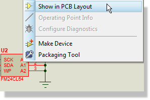
1. Right click on the schematic component and select 'Show in PCB Layout' from the resulting context menu.
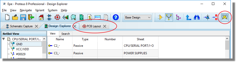
2. From Design Explorer, click on the part or net that you want to view
in the PCB package, make sure that the Cross Probe icon is selected and
click on the ARES tab.
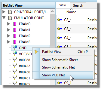
3. From Design Explorer, right click on the part of net that you want
to view in the PCB package and then select either Show PCB Part or Show
PCB Net as appropriate from the resulting context menu.
Live Cross Probing
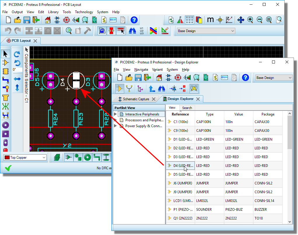
You can automate navigation to both schematic and layout modules by switching on the live cross-probing mode.

When enabled the clicking on an component in Design Explorer automatically tags the component part on the schematic and/or the footprint on the layout.
The difference between live mode and those described above is that there is no automatic switch of tabs in automatic mode. The most useful way to cross-probe in this way is therefore to detach the design explorer from the frame containing the schematic/layout (drag the tab and drop it). With the design explorer is a separate frame you can then click on a component and view the corresponding schematic/layout.
See Also: