Board Stackup Wizard
Overview
This dialogue configures the layer stackup for the PCB including the construction method, materials, thicknesses and dielectric constants. It is launched from the Stackup Wizard button on the Layers tab of the layer stackup dialogue, and it also appears as a page of the New Project Wizard.
The information provided here is used by Proteus in several ways:
- The number of layers and the board style together determine the legal set of drill passes for the PCB. This governs the types of via that can be placed during manual and auto-routing.
- The number of layers determines the set of layers available in tracking mode.
- The thickness parameters are used when length matching to calculate via length contributions to the routes.
- The entire stackup information is exported in the CADCAM readme file so that your board manufacturer is aware of your intended design.
A quick way to construct a stackup for a standard 1.6mm board is to choose from one of our generic templates in the New Project Wizard. If you do so, make sure you understand about plane layers as you may need to change the layer types to accommodate your particular PCB.
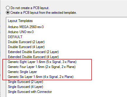
Generic 1.6mm (+/- 10%) PCB templates for different numbers of copper layers.
Options
Template
The Template group holds the two choices that shape everything else: the board style and the number of copper layers.
Board Style
For multi-layer boards this choice determines the manufacturing construction method. The three available styles are:
- Internal Layers, where the stackup is built from the inside out starting with a central core. Additional layer pairs are added outward using pre-preg and copper foil.
- External Layers, where the stackup is built from the outside in using multiple individually drilled and plated cores bonded together with pre-preg.
- 1+n+1 HDI (single buildup), High Density Interconnect construction using a conventional core with one laser-drilled buildup layer on each side. Micro-vias connect the outer copper to the first inner layer only.
The board style directly determines which drill spans are valid and therefore which types of via can be placed. The drill constraints and engineering trade-offs for each board style are discussed in detail in the main Manufacturing and Cost Considerations topic.
No. of Copper Layers
Specify the number of copper layers on the PCB. Available values are 1, 2, 4, 6, 8, 10, 12, 14 and 16. This count includes any layers that will be designated as plane layers.
Materials
The materials section specifies the composition of each construction element. Under normal conditions the core is almost always FR4 laminate and the soldermask is LPI (Liquid Photo Imageable). For high-frequency RF/analogue or high-speed digital designs, specialist materials with different loss tangent and dielectric properties may be required.
- Solder Mask, the material for the soldermask layers. Default: LPI.
- Core, the laminate material for core layers. Default: FR4.
- Buildup, the material for HDI buildup layers. Default: RCC (Resin Coated Copper). Only enabled when the 1+n+1 HDI board style is selected.
Specifying a change of material is likely to affect the dielectric constant values and may also influence available thickness options from your fabricator.
Material information is exported in the CADCAM readme file for the board manufacturer. You can safely leave the default values if this is not relevant to your project.
Thickness
The thickness section specifies the physical dimensions of each construction element. The heading of the group carries a running total of the resulting board thickness, which updates as you type.
- Solder Mask, the thickness of the soldermask layer applied over the outer copper. Typical range: 0.3th to 1.5th (8 to 38 µm).
- Core, the thickness of each core laminate layer. Typical range: 4th to 62th (0.1 to 1.6 mm). Standard cores for a 1.6 mm two-layer board are around 60th (1.5 mm); inner cores on multi-layer boards are typically 8th to 20th (0.2 to 0.5 mm).
- Prepreg, the thickness of each pre-preg bonding layer. Typical range: 1.4th to 8th (35 to 200 µm).
- Inner Copper, the thickness of inner copper layers. Typical range: 0.5th to 2.8th (12 to 70 µm). Standard 0.5 oz copper is approximately 0.7th (18 µm) and 1 oz is approximately 1.4th (35 µm).
- Outer Copper, the thickness of outer copper layers. Typical range: 0.5th to 5.5th (12 to 140 µm). Outer layers are often thicker than inner layers due to electroplating during the through-hole plating process.
- Buildup, the thickness of HDI buildup dielectric layers. Typical range: 1.5th to 4th (40 to 100 µm). Only enabled when the 1+n+1 HDI board style is selected.
These values are used by Proteus to calculate via depth for length matching and are exported in the CADCAM readme file. You can safely leave the default values if accurate via length calculation and manufacturing data are not important for your project.
The ranges quoted above are fabrication guidance rather than limits imposed by the dialogue, which will accept any value you enter. They are typical for mainstream PCB fabrication; always confirm the actual available thicknesses with your board manufacturer, as these vary between fabricators and depend on the specific laminate system in use.
Dielectric Constants
The dielectric section specifies the relative permittivity (εr) of each insulating layer. These values are important for impedance-controlled designs and are exported in the CADCAM readme file.
- Solder Mask (εr), the relative permittivity of the soldermask. Typical range: 3.0 to 4.0.
- Core/Prepreg (εr), the relative permittivity of the core and pre-preg layers. Typical range: 3.8 to 4.8 for standard FR4, measured at 1 GHz. Lower values (3.0 to 3.5) are typical for high-frequency laminates.
- Buildup Layer (εr), the relative permittivity of the HDI buildup dielectric. Typical range: 3.0 to 4.0. Only enabled when the 1+n+1 HDI board style is selected.
Dielectric constants vary with frequency, temperature, and resin content. The values specified here should correspond to the operating frequency of your design. Consult your laminate supplier's datasheet for accurate values at the relevant frequency.
See Also: