COMPONENT PLACEMENT
Component Placement
A netlist is a set of information about components and how they are connected (wired up), used to transfer information between a schematic module and a PCB layout module.
Proteus 9+ works with a live netlist, so the layout module already has much of the information we need to start the layout process (having automatically received this from the schematic module). In particular, we have specified which footprints are associated with each schematic symbol and so Proteus can therefore pre-select these for us ready for placement. This brings us to an important distinction in the software; the difference between a component and a package.
Components and Packages
- A component is an instance of a footprint that has been netlisted through from the schematic.
- A package is a physical footprint that exists in the PCB Layout Libraries.
- The component "Capacitor C1" has an "0805" package, for example.
More information on the Libraries can be found here.
Selecting component mode will bring up a list of parts (received from the schematic via the netlist) which still need to be placed on the PCB (similar to the list of parts in the Bill of Materials); Proteus also knows how these parts should be connected (wired up), again having received this information from the schematic module.
Selecting package mode will access ‘unconnected’ physical instances of a footprint. This mode is only really useful when wanting to modify an existing footprint, or perhaps check some detail on a particular footprint; when working with a layout which is driven from a schematic we therefore typically only use component mode.
The Component Mode icon is second from the top directly underneath the Selection mode icon. Clicking on this will display a list of items in the Object Selector which correspond directly to the parts on the schematic.
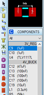
Component Mode
The Package Mode icon is directly underneath the Component mode icon and clicking on this will show us the physical footprints corresponding to the components in the layout.
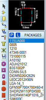
Package Mode
When placing, routing and laying out a PCB based on a schematic (as is usually the case, and as is the case with this project) then we will be working with Component mode.
The Board Edge
Before we can place the components on the board we need to define what shape and size the board will be. For our project we only really need a simple rectangular board edge, but we can optionally round the edges for a little more practice.
The first thing to point out here is that the layout module will operate in either imperial or metric units and you can switch between modes either by toggling the Metric command on the View menu or via the ‘M’ keyboard shortcut. You may need to switch units for the placement of the board edge and also elsewhere in the documentation.
You can set your default or preferred units from Technology Menu - Set Grid Snaps command. The grid granularity can also be set here.
First we will place a simple rectangular board edge, measuring 65.5x65.5mm. The first thing to do is check that we are in Metric mode and set our grid snap to 0.5mm (View menu). Then select the 2D Rectangle icon from the left hand side of the application.
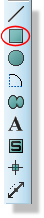
2D Rectangle Icon
Next, change the Layer Selector to the Board Edge Layer.
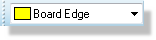
Board Edge layer selected
Move the mouse to the approximate starting point for the board edge (e.g. bottom left). Now, hold the mouse still and press the ‘O’ key on the keyboard to set the origin of the co-ordinate system to the point under the mouse (alternatively, you could start the rectangle from the 0,0 point in the default co-ordinate system). The false origin (if set) will be reflected in the co-ordinate display at the bottom right of the application. Left click to start placement and drag in the normal way. The co-ordinate display at the bottom will show you the dimensions of the board edge as you drag.
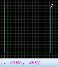
Drawing a board edge
The ‘M’ key on the keyboard can be used to toggle between metric and imperial units as required whilst drawing, and the 'Ctrl+F1'/'F2-F4' keys can be used to change the grid snap. Once you have the desired size of board edge click left again to commit placement. You don’t necessarily need to worry about where in the Editing Window you have placed the board edge, as we can always move it to the centre of the world area (this will be detailed shortly).
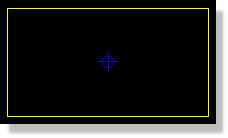
Placed board edge which is always Yellow
If you would like to easily enter a specific size for the board edge using the keyboard, then Edit the board edge graphic (right click, Edit Properties) and set the dimensions to your requirements:
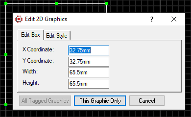
Setting the dimensions of the board edge
Finally, restore the co-ordinate system to it’s global origin again (if a false origin was specified) by pressing the ‘O’ button on the keyboard again. The colour of the co-ordinates will be magenta if a false origin is in use and black if the global origin is in use.
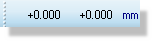
Co-ordinates at 0,0
Placing a board edge should always be the first task as the software needs to know the boundaries of the board in order, for example, to know the limits of where the autorouter can function or the size of a power plane.
If you need to delete the board edge or resize it you can do so via the context menu options and drag handles that will appear when you right click over the board edge graphic.
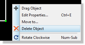
Select Delete from the context menu
Board Edges of any complexity are best brought in from the MCAD tool via the Import DXF command on the File Menu (and placed onto the board edge layer!)
See Also:
In order to draw a board edge with curved corners we can use the "2D Graphics Closed Path Mode". Note that this step is optional and can be skipped if you prefer.

2D Closed Path Icon
We will round the edges of the board with a 4.5mm radius. First delete the rectangular board edge, then start a closed path from a point (0mm,4.5mm) from the origin (global origin or false origin, it doesn't matter). Then hold down the CTRL key to enter arc mode and drag the mouse around to (4.5mm,0mm) and click again (note that the direction of mouse dragging determines the direction of the arc).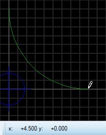
2D Closed Path Curve
Release the CTRL key in order to add a straight line segment, move the mouse to (61mm,0mm), and click again.
2D Closed Path Curve to Line
Repeat this process for the rest of the rounded rectangle in order to complete the closed path (co-ordinates will be a variation of 0, 4.5, 61 and 65.5). When you click back on the start point of the path then it will close and complete.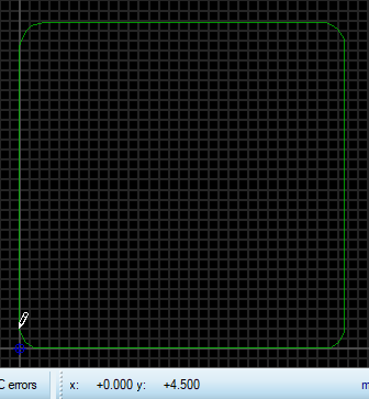
Completing the 2D Closed Path
You may actually find it helpful to leave the original rectangle in place in order to aid the drawing process (the undo button can be used to restore the rectangle if it was deleted), deleting it afterwards. Note that it is also possible to piece together a board edge from individual line and arc segments drawn separately, using the line and arc modes, so long as these touch exactly on their ends (if they do not touch exactly then they will not be considered a complete board edge by Proteus).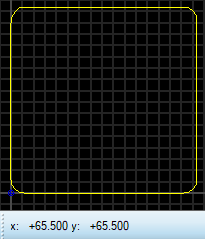
Completed Rounded-Rectangle Board Edge
Layer Stackup and Drill Spans
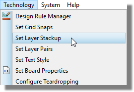
As part of the schematic tutorial, we set the board layer stackup and drill spans using the New Project Wizard. If you should have a need to review/change these at a later stage then this can be done using the Set Layer Stackup command on the Technology menu.
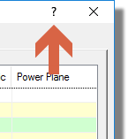
Note that dialogue level help is available should you need it, and if you are unsure about anything then the topic is discussed in detail in the reference manual.
See Also:
Reference Manual : About Layer Stacks
Reference Manual - About Drill Spans
Reference Manual - Specifying Plane Layers
Work Area, Co-ordinates and Snap
It is likely that your board edge covers a small portion of the Editing Window, which is less than ideal as all of the work will be taking place inside this area. We can of course zoom into the area (point the mouse and roll the middle mouse button or use the F6 key) but the default zoom level is designed to show the entire Work area. The Work area is the area inside the dark blue box at the edges of the Editing Window. Let’s tidy this up a bit before we move on.
Start by switching into Selection Mode and then left click and drag a selection box around the board edge.
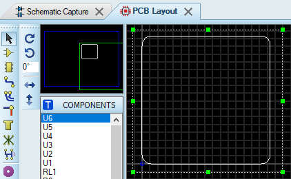
Selection mode and the board edge selected
If you get it wrong and don’t completely cover the board edge, use the green handles to resize the selection box until it completely encompasses the board edge.
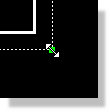
Resizing a box by the drag handles
Now place the mouse inside the selection box, depress the left mouse button and drag into the centre of the work area, releasing the mouse button to commit the placement.
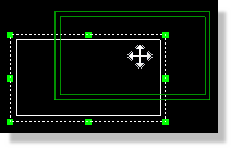
Moving the board edge
Block selection is a very important technique worth mastering as it allows you to easily select and then perform actions on (move, delete, etc.) groups of objects.
Having centred our board edge in the Work area we can shrink the work area to a suitable size. From the Technology Menu, select the Board Properties command and then set to something like 100mm by 100mm, such that the resulting work area forms a reasonable boundary to the board.
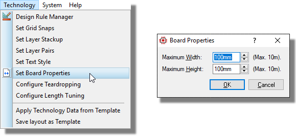
Setting the board properties
Move the board outline again if necessary to get it to the centre of the work area.
We saw briefly when placing the board edge that we can specify a temporary origin and use that to place items of a given size (or to place items a specific distance away from our origin point for example). We can however, also specify the location of the Output Origin. This is the default origin used whenever we do not explicitly set a temporary origin and is shown on the layout as a small blue marker.

It can be useful to move this to a corner of the board and particularly so if we have mechanical constraints that we need to consider during placement (e.g. mounting hole locations). For our design, we’ll move the origin to the bottom left corner of the board edge.
1) From the Output menu choose the Set Output Origin command.
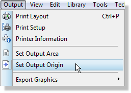
2) Move the mouse towards the bottom left of the board edge. Roll the middle mouse button as required to zoom in for more accurate placement.
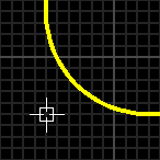
3) Left click the mouse to commit placement.
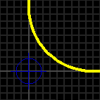
The co-ordinate display will now provide values relative to the position at the bottom left of the board by default, and relative to any specified temporary (false) origin when set.
Remember that you can also toggle metric or imperial units via the command on the View menu or the ‘M’ keyboard shortcut.
A useful trick once we have specified our origin is to use the Goto-XY command on the View Menu to move the mouse to the exact location we want to place position sensitive parts. This command will automatically switch between X-Y or Radius-Theta depending on whether you are in polar or cartesian co-ordinates.
The Proteus layout module has a default grid and will snap objects onto the grid, making it easy to form connections and control board layout. There are four hotkeyed snap settings for both metric and imperial units, changeable from the View Menu or by keyboard shortcuts. It follows that changing the snap setting to a lower unit will allow finer granularity, whereas raising the snap setting will make it easier to select objects at higher zoom levels. It is not advisable to change the snap settings regularly through a design but rather to choose the highest appropriate setting for the board you are working on.
You can change the four default snap settings via the Grids command on the Technology Menu:
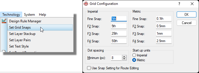
Grid settings can be set according to the users requirement
The grid display itself can be toggled between off, dots and lines via the ‘G’ key on your keyboard, whilst the colour of the grid can be configured from the Displayed Layers Dialogue (View Menu).
Mounting Holes and Pad Styles
Next we will place some mounting holes on our board. Mounting holes could be added at any stage of board design; if the mounting holes must match a specific enclosure then they will typically be added before placing components, otherwise they could be added after placing components depending on where they fit best. In our case we will place the mounting holes first at the edges of the board, as well as one hole near the centre. We will use a pad with a 3.2mm hole and a diameter of around 6.2mm. The first thing we need to do is switch into circular through hole pad mode and scan for a suitable pre-supplied pad in the Object Selector.
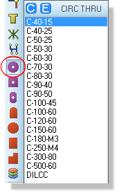
Select the correct pad style for mounting holes
The nomenclature of pads is designed for easy reading and tends to follow the following format:
<PAD TYPE> - <DIAMETER/SIZE> - <HOLE>
Units are in imperial unless prefixed with an ‘M’ so for example a C-40-15 is a circular pad with a 40th diameter and a 15th hole and a C-200-M3 is a circular pad with a 0.2in diameter and a 3mm hole. Our spec requires a pad with a 6.2mm diameter and a 3.2mm hole, which we can see does not exist in the pre-supplied set. We therefore need to create the pad as follows:
1) From the Library Menu select the New Pad Style command.
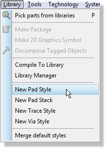
2) Enter a name for the pad; we recommend you follow the standard naming convention (i.e. C-M6.2-M3.2).
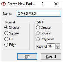
3) Specify the pad type – in our case we want Circular through hole pad.
4) The diameter of the pad is 6.2mm.The drill mark is the size of the mark output in a drill plot, 10th would be fine. The drill hole needs to be 3.2mm and the guard gap should be enlarged to 10th The guard gap (or solder mask expansion) is the amount by which the pad diameter is expanded on the resist plot.
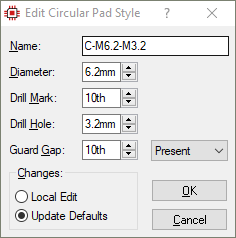
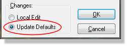
5) At the bottom of the dialogue form we have the choice whether to make this pad style permanent for future designs (Update Defaults option) or local only to this design (Local Edit option). Unless there is a particular reason for a local edit only we recommend that you leave this on the default setting.
6) When you exit the dialogue form you should see that the new pad style is available for placement from the Object Selector.
When entering specific values you may find it easier to simply type in the values that you want rather than using the up and down arrows beside the controls.
We are going to want a mounting hole at each corner of the board, and then another one at a specific position near the centre of the board. With circular through-hole pad mode selected, choose the C-M6.2-M3.2 pad style and place one at each corner of the board (the co-ordinates will be a variation of 4.5mm and 61mm).
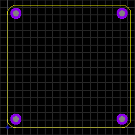
Corner mounting holes placed
We want to place the next mounting hole at (32.75mm,39.5mm). This may be challenging using the grid, so we will simply place it nearby and then enter it's exact position using a dialogue. Place the mounting hole somewhere near the middle of the board, then right click on it and select "Move To..." from the context menu.
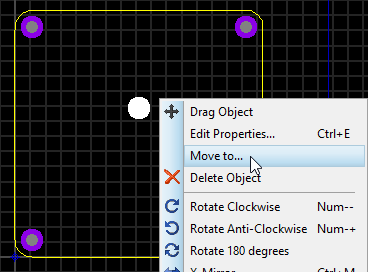
Moving a mounting hole to a precise location
In the dialogue, enter 32.75mm, 39.5mm and then click OK.
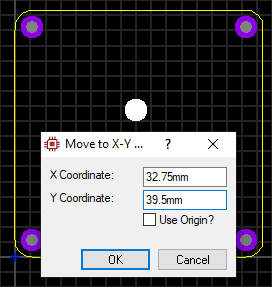
"Move to" dialogue
With position-sensitive components it is often useful to ensure that they cannot be nudged or moved inadvertently after placement. You can lock any object in position by moving the mouse over the object until it is encircled by a dashed line, right clicking on the object and selecting Edit Properties from the resulting context menu. The Lock Position checkbox can then be selected to prevent movement or deletion of the part.
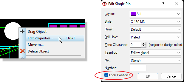
Locking pads and components
You can also set a specific minimum zone clearance for the pad to reserve some extra space for the bolt.
Placing Components, and The Ratsnest
Now that we’ve handled all the basics we can finally start to get our components on the board.
Towards the end of the schematic tutorial, we placed certain components in groups; such as grouping decoupling capacitors together with the components which they should be placed nearby to. We will now draw "placement rooms" on the PCB for these groups. Start by selecting Room Mode:

Room Mode
Draw placement rooms in the approximate locations shown, and assign them to the appropriate groups as shown.Clicking point by point will create a polygonal room shape, whilst clicking and dragging will create a rectangular room shape.
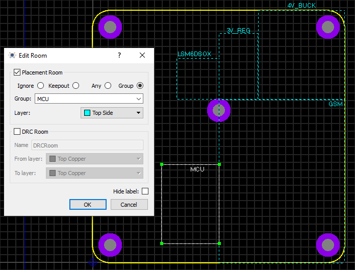
Room Mode
Placement rooms only need to be approximate as we will move components around after placement. Placement rooms should not however overlap.If you don't want to draw all the rooms, then you can load the "IoT Pump (Placement Rooms)" sample design.
Next, we will use the auto-placer to place most of the board components in approximate locations. Select "Auto-placer" from the Tools menu and enter 40th for the Placement Grid, 1th for the Edge Boundary, and Push & Shove on. Then click the "Schedule" button to arrange components from largest to smallest, before clicking "OK" to start the Auto-placer.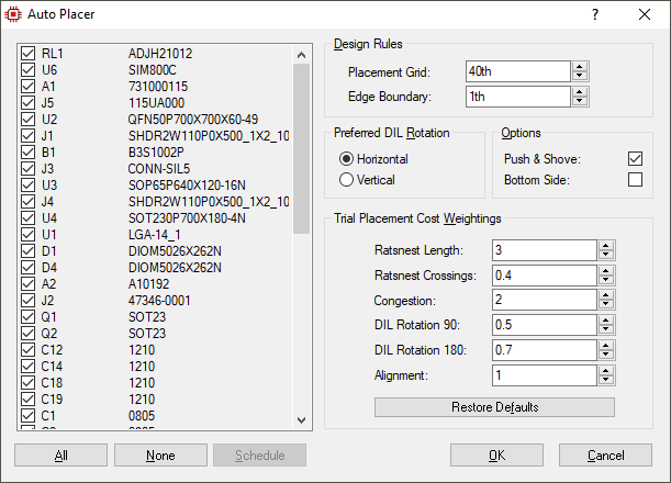
Auto-Placer
See Also:
Auto-placement and Floorplanning
Once the auto-placer completes, you will notice a lot of green and yellow lines drawn amongst the placed components; the green lines are the "ratsnest lines" and the yellow arrows are "force vectors".
If you do not see the "force vectors" by default then they can be turned on by selecting "Edit Layer Colours/Visibility" from the View menu. Select the "Force Vectors" check box to turn them on (located in the Other Colours tab). Note that similar steps can be followed to remove the "force vectors".
If you see a lot of DRC errors - indicated by red circles - then don't worry, we will adjust the DRC rules to clear these in a following section. The DRC checker can be turned off temporarily by selecting "Design Rule Manager" from the Technology menu, deselecting "Enable design rule checking?" at the bottom of the dialogue, and then clicking OK; we will adjust the rules and re-enable the DRC before routing the board (alternatively, just change the DEFAULT Pad-Pad clearance to 7th).
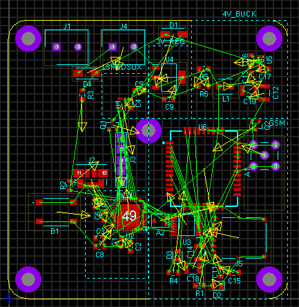
Auto-Placed Components
The green ratsnest lines indicate wiring connections which still need to be made (by placing tracks or zones to join them). The yellow force-vector arrows indicate approximately where a component should be placed in order to minimise the length of the ratsnest lines attached to it (this is just a guide, components are rarely ever placed exactly where the force-vector indicates).
The number of "missing(s)" displayed in the status bar corresponds to the number of remaining ratsnest lines (connections which still need to be made).
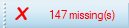
Once we have completed the design, there should obviously be no more "missing(s)" and we should see a green tick here with a "No CRC errors" message.
If you should find the ratsnest lines and force vectors distracting (at least initially) then you can turn them off using the Colours and Display Settings dialogue:
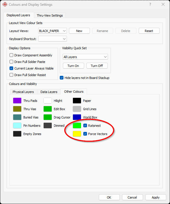
The Ratsnest and Force Vector layers turned off
See Also:
Ratsnest Features (Reference Manual)
The auto-placer will place most of the components, however as our board is a bit tight it may not place all of them - this is no problem, as we will quickly place the remaining components manually. Most likely the relay, RL1, was not placed. We will make a little space for it on the left of the board and place it manually (if it was placed on your board then you can simply delete it in order to follow along). Move components as necessary in order to clear a space to the left of the MCU / LSM6DSOX rooms; components can be placed outside of the board edge for now if necessary. Moving of components can be done using the techniques covered in the schematic tutorial as well as earlier in this tutorial.
Once a space has been cleared then select Component Mode, select the relay from the Object Selector, and rotate it as shown:
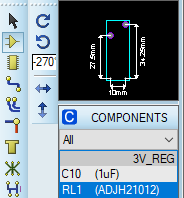
Selecting and rotating the relay
Also check that the layer is set to Component Side (top side):

Component Side layer
Next we will place the relay on the board. Similar to the schematic, click once to get a preview of the component to be placed, then move it into position and click again to commit the placement. Note that the preview can be rotated using the + and - keys, and the grid snap can be changed using the Ctrl+F1 / F2-F4 keys.
Placing the relay component
Place any other components which may remain. Next, we will quickly cover another two placement methods: Placement by Room, and Placement by Tagged. As we have already placed all our components we don't need to use these, however they are worth covering for future reference.
Placement by Room
Delete all components in the MCU room in order to add them back to the component list (object selector). You may find the selection filter helpful for ensuring that only components are selected and not the room itself. Next, right-click on the group header in the component list and select "Place Group by Room" from the menu.
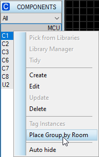
Place Group by Room
This is similar to using the auto-placer, but just for a single placement room.
Placement by Tagged
The "Placement by Tagged" feature enables you to filter the component list (object selector) by selecting certain components on the schematic. Again delete the MCU components, then go to the schematic and tag the MCU decoupling capacitors.
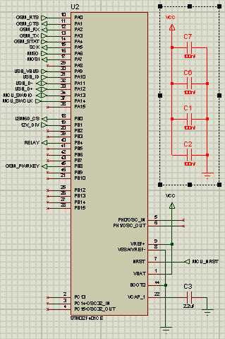
MCU Decoupling Caps Tagged
Go back to the PCB layout, and select "Tagged" from the component list dropdown - only tagged component tagged on the schematic will then be listed.
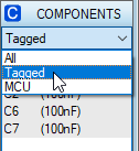
Filter component list by tagged components
Place the components again, or undo, so that all components are again placed on the board.
Component References and Values
Component references (IDs) and values are fully flexible and we can move, rotate, resize and hide them independent of the component itself. We can also set the font from the Technology menu (Set Text Style). Component references are visible by default, whilst component values are hidden by default. In order to hide or show a component reference / value, right-click on the component body (not the reference / value text) and select "Edit Properties...", then use the "Hidden" tickboxes. Note that you can also change the component reference / value from here and the change will automatically be back-annotated to the schematic.
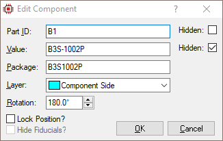
Edit Component Dialogue
To change a component reference / value rotation or size; right click on the reference / value label and then select "Edit Label".
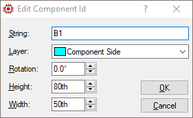
Edit Component Label Dialogue
Similar to the schematic module, if you move a component body then the reference / value will move along with it, however if you move the component reference / value labels then these will move independently of the component. Try moving the B1 button label reference to the right of the button, for example.
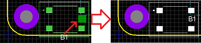
Moving a component reference
Arranging Components
Next we will arrange the components on the board to approximate locations. Again, this can be done using the various options and techniques already learned (block move, tag-and-drag, right-click drag, block rotate, right-click rotate, etc).
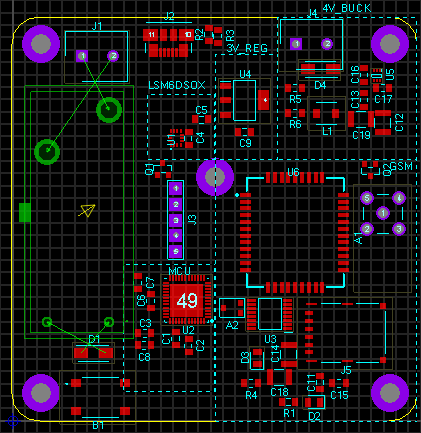
Arrange the components and labels as per the below graphic. You also have the option to practice arranging a few components if you like, and then just load the pre-supplied sample design which has all the components placed ("IoT Pump (Components Placed)").
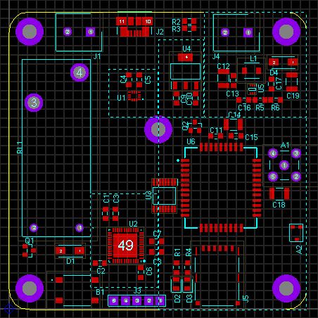
Components placed and positioned
The following points are useful to bear in mind as you continue placement:
- The middle mouse will zoom you in and out as you place components (as will keyboard shortcuts F6 and F7)
- Right clicking on a component once placed will present a context menu option, allowing you to move, rotate or delete the part.
- Changing the snap settings to a finer grid will allow more accurate positioning at the expense of more precision being required to select the part.
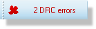
- If you place a part in an illegal position (e.g. over another part), and DRC has not been turned off, then you will get one or more design rule violations.
DRC errors