DESIGN RULE SETUP
Design Rules and Net Classes
Now that we have a placed board we need to use tracks to link everything up. Before doing so, we will configure the track widths and clearances using a dialogue called the Design Rule Manager. Start by launching this dialogue form now from the Technology Menu in the Proteus Layout module.
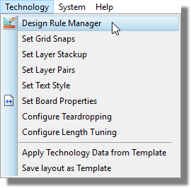
Design Rules
The first tab of this dialogue form allows us to configure constraints and minimum clearances for the layout. We have a DEFAULT rule loaded which must apply to all layers and all net classes, providing a set of clearances between objects equivalent to manufacturing guidelines.
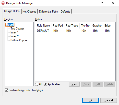
The Design Rule Manager
This rule and these clearances are created automatically for each layout in order to provide a minimum set of constraints for a board.
The first thing we need to decide is whether a single rule is suitable for all layers and all traces on the layout. It is possible to create as many new rules as required and we can limit their effect to a given layer on the PCB, a specific area of the PCB and/or a given set of connections (net class). A great deal of information on this is available in the reference manual, and we will cover a few of the potential scenarios in this tutorial.
As a number of the components on our board already have Pad-Pad clearances which are smaller than the default 10th setting, the first thing which we will do is adjust the default Pad-Pad clearance down to accommodate this. Select the DEFAULT rule and click the "Edit" button, then change the Pad-Pad clearance down to 7th before clicking OK.
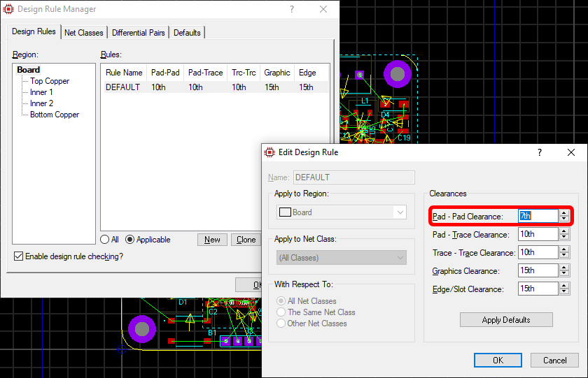
Default clearance settings in the DRC manager
The Pad-Trace, Trace-Trace, Graphics and EdgeSlot clearances are fine at the default values.
Note that the edge/slot clearance field defines the clearance for power planes against the board edge.
If you disabled design rule checking earlier in this tutorial, then be sure to enable it again now by checking the "Enable design rule checking?" box.
As our relay switch tracks will carry the relatively high voltage of mains power, we will want to give these some additional clearance to avoid arcing. Create a new design rule at the Board level and give it any sensible name, e.g. RELAY_SW. We want this rule to apply to the whole board, with respect to our RELAY_SW class (which we set on our relay switch tracks on the schematic by applying wire labels to them), with clearances of 50th throughout.
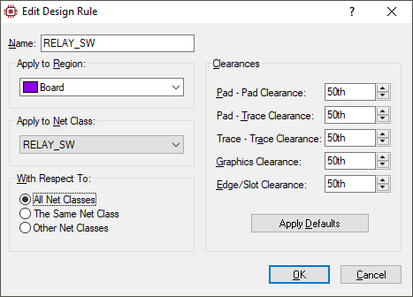
Rule for the RELAY_SW class
In addition to these clearances there is a board global rule for Resist-Trace clearance. This rule enforces a clearance between the solder mask and copper and is intended to prevent exposed slivers of copper on the manufactured PCB.
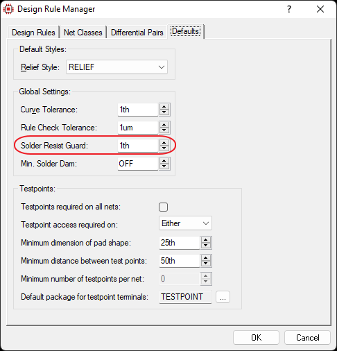
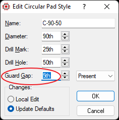
If, during route placement, you find these DRC errors, the solution is to either move the trace or edit the pad style and change the guard gap (solder mask expansion) for that pad style.
We will move onto the Net Classes tab for now, but we will come back to the Design Rules tab a little later.
See Also:
Setting Design Rules (Reference Manual)
Design Rule Examples (Reference Manual)
Net Classes
This is the place where we configure trace and via styles and control which layers we route on when auto-routing the board. The selector at the top allows us to switch between different net classes and configure each separately.
Proteus contains the SIGNAL class by default, and any nets which are not specifically assigned to a class (and are also not POWER nets) will automatically be assigned to this class. Any nets which are connected to a POWER or GROUND terminal will be assigned to the POWER class by default. The other net classes present in the list are the ones which we specifically created on the schematic by assigning CLASS=xyz wire labels to their wires.
Let’s start with the POWER Net class. We’ll set the track / trace size to 20th, to assist with current-carrying capacity and also to reduce track impedance (we’ll also place low impedance ground planes later to help with this). In Proteus nomenclature this corresponds to track style T20.
In order to get these thicker tracks routed into our finer-pitch components, where things are more congested and 20th tracks simply won't fit, we will set a Neck Style of DEFAULT (which is 10th). Track necking (thinning) is a feature whereby tracks may jump to a different size under exceptional circumstances, such as to pass through obstacles. Together with our design rule aware routing (which knows which objects are obstacles) this is very powerful. When set, you can hold the SHIFT key during route placement to toggle between necked and normal track styles which is invaluable in tricky or dense routing.
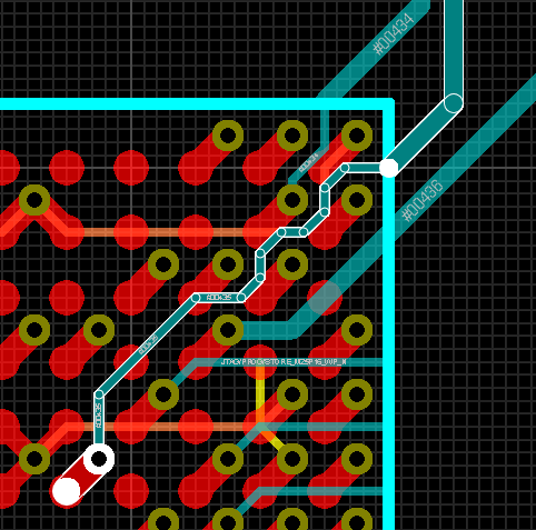
Advanced necking: The SHIFT key is held down while routing the escape from the BGA and then released to resume routing at normal track width.
We will stick with the default Via Style.
If you are not sure of the characteristics of a particular style, you can view them by selecting the appropriate mode icon (via, track, pad, etc.), highlighting the style in question in the Object Selector, and then clicking on the ‘E’ button at the top of the Object Selector.
The remaining options on the left of the dialogue form allow us to optionally select different trace and neck styles for the inner layers, choose between Smart and Thru-Hole vias and optionally select a different colour for this net class's ratsnest lines (or hide them entirely). If the Smart via type option is selected then the autorouter will automatically use blind/buried vias where appropriate. Changing the colour of the ratsnest lines can be useful if we are manually routing and wish to quickly distinguish between power and signal connections, or even highlight high-speed lines.
On the right side of the dialogue is the layer assignment for autorouting. We can use these settings to restrict certain net classes to specific layers, as well as to tell the autorouter to prioritise certain classes over others. As our bottom layer is a Plane layer (no tracks allowed), we need to tell the autorouter to use the Top Copper, Inner 1 and Inner 2 layers for routing; select Top Copper and Inner 1 for Pair 1, and Inner 1 and Inner 2 for Pair 2.
We should now have finished setting up the POWER net class – your dialogue form should now be configured as per the following screenshot.
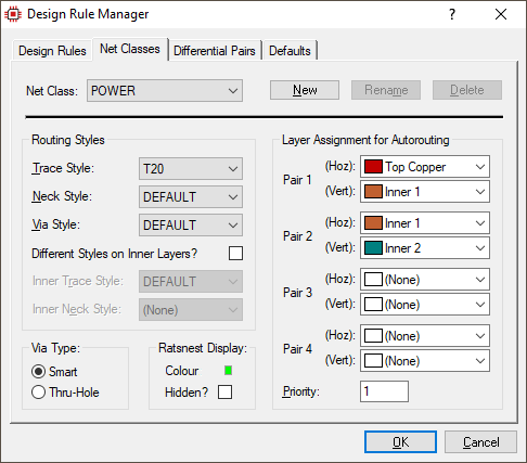
Specifying the POWER net settings
Let's now do the settings for the remaining net classes. All net classes should use the Autorouting Layer Assignments already specified, and the routing styles should be as follows:
| Net Class | Trace Style | Neck Style | Notes |
| POWER | T20 | DEFAULT | Thicker traces for power tracks. |
| 50_OHM | T20 | (None) | Trace thickness calculated (using an external tool) for 50 ohm impedance. |
| RELAY_SW | T80 | (None) | Thicker traces for relatively high-current relay switch tracks. |
| SIGNAL | DEFAULT | T6 |
Creating your own net classes on the schematic is extremely simple and provides you with the flexibility you need both with regard to trace and via configuration but also with design rule constraints
See Also:
Net Classes (Reference Manual)
Design Rule Rooms
We have set our board-level Pad-Pad clearance rule to 7th in order to accommodate our fine-pitch components. Our Pad-Trace and Trace-Trace clearances are still set to 10th however, so when we start trying to route tracks into and around our fine-pitch components then we will likely start running into Pad-Trace and Trace-Trace DRC problems. We could set the board level values for these rules down in order to resolve the problem, however if we would like to keep greater clearances on our board in general but allow tighter clearances within a specific area (such as around a fine-pitch component) then we can use the DRC Room feature to accomplish this. Using this technique, we will need DRC Rooms around our MCU, the IMU and the DC-DC converter (the DRC rooms in the following image are the red dashed rectangles around the highlighted components).
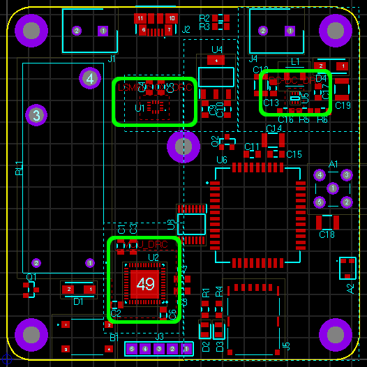
DRC Rooms (red dashed rectangles)
To draw a DRC room, select the Room Mode tool (the same as what we did for the placement rooms).
Room Mode
Draw a room around the relevant component, but this time select the "DRC Room" option.
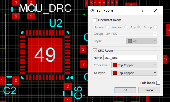
Edit Room
Draw rooms for the MCU, IMU and DC-DC Converter (using names such as "MCU_DRC", "LSM6DSOX_DRC" and "DC-DC_DRC"). Our rooms only need to apply to the Top Copper layer of the board (where our fine-pitch SMD components are placed).
Clicking point by point will create a polygonal room shape, whilst clicking and dragging will create a rectangular room shape. The auto-router currently only supports rectangular DRC rooms.
Next go back into the Design Rule Manager and you should see the new DRC rooms listed under the Top Copper layer. Select each room and create a rule for it, with 7th clearances on Pad-Pad, Pad-Trace and Trace-Trace.
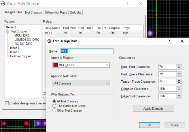
Edit DRC Room Rule
Design Rooms are a really useful concept and helpful wherever clearances vary in specific regions of the PCB. This can be as simple as pad-pad clearance on fine pitch SMD devices, fanout areas from BGAs, edge connectors at the board edge and so on. We strongly recommend you read up further in the reference manual.
Differential Pairs
Differential pairs functionality is included in the Advanced Feature Set and requires a license for PCB Design Level 2 or higher.
The last thing which we need to do in terms of design rule setup is to handle our differential pair rules for the USB. Using an external tool (such as a website or the Saturn PCB Toolkit) we calculated our track thickness at 10th and our track separation at 12th for a 90ohm differential impedance on our Inner 2 layer.
In the Design Rule Manager, go to the Net Classes tab and create a new net class called "USB", giving it a Trace Style of T10.
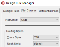
USB Net Class
Next go to the Differential Pairs tab and assign the USB Net Class to the USB Diff Pair. Set the Min Paired Separation to 12th, the Max Unpaired Length to 0.2in and the Max Phase Shift to 15th.
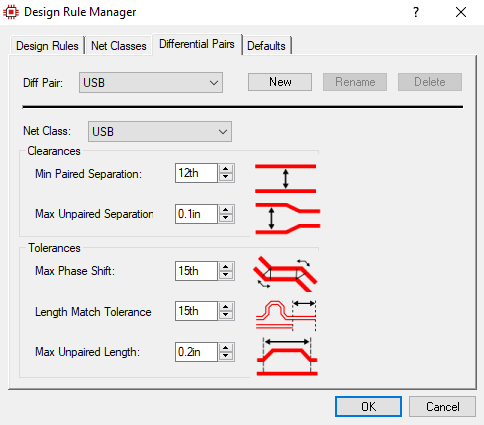
Differential Pair Setup
Next go to the Design Rules tab and create two rules:
1. A Board-level rule, called USB_PAIR_RULE_1, which enforces the 12th Min Paired Separation by have a Trace-Trace Clearance of 12th. This rule should apply to the USB net class with respect to itself ("The Same Net Class").
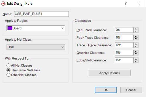
Differential Pair Spacing Rule
2. A rule on the Inner 2 layer, called USB_PAIR_RULE2, to keep other tracks well clear of the USB differential pair by enforcing 20th Pad-Trace and Trace-Trace clearances. This rule should apply to the USB net class with respect to other net classes.
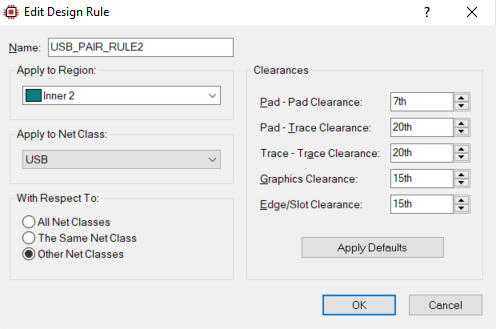
Differential Pair Clearance Rule
Click "OK" to close the Design Rule Manager once done.
See Also:
Layer Pairs
On 2-layer boards, any vias will obviously go between Top Copper and Bottom Copper. On multi-layer boards, we can instruct Proteus regarding which layer to jump to by default when placing a via from another layer during manual routing. On our board, for example, the Bottom Copper layer has been set as a "Plane Layer" (for impedance-control reasons) and we do not wish to route any tracks on it - when placing a via from the Top Copper we will therefore not want to jump to the Bottom Copper by default (in fact, Proteus will not even allow this due to the Bottom Copper being a Plane layer), but rather to one of the inner layers. To set this up, launch the "Edit Layer Pairs" dialogue by selecting "Set Layer Pairs" from the Technology menu.
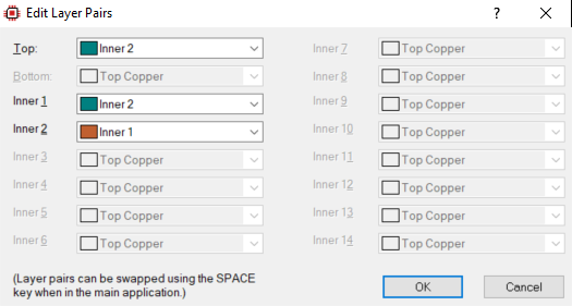
Layer Pairs Dialogue
Change the Top layer pair to be Inner 2. When we start placing a via from the Top Copper during manual routing then the layer selection will change to the Inner 2 layer by default (note that this is only the default and we can of course select a different layer at that stage if we wish). Inner 1 can stay paired with Inner 2 and vice versa as per the defaults; when we place a via whilst routing on the Inner 2 layer then the layer selection will change to the Inner 1 layer and vice versa.
See Also:
Length Matching
Length matching functionality is included in the Advanced Feature Set and requires a license for PCB Design Level 2 or higher.
Length Matching can be setup in the "Length Matching" dialogue by selecting "Configure Length Matching" from the Technology menu.
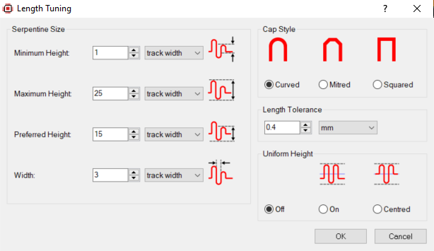
Configuring Length Matching Options
The default settings will be fine for our application, so no changes are needed here.
Teardrops
Teardrop functionality is included in the Advanced Feature Set and requires a license for PCB Design Level 2 or higher.
Placing teardrops at the connection point between track and pad is often useful in preventing drill breakout during board manufacture. We can configure teardrops from the Configure Teardropping command on the Technology Menu.
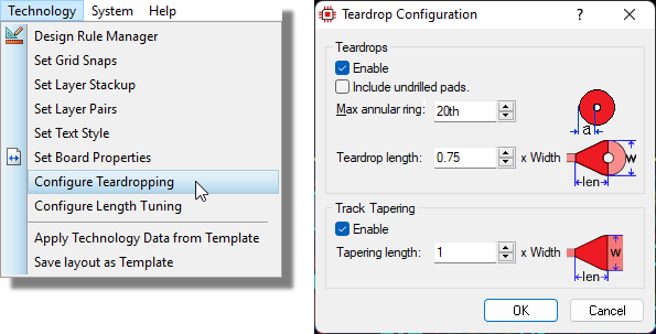
The dialogue form lets us set the maximum annular ring size on a pad below which a teardrop connection will be made and then also lets us set the length of the teardrop. You can, if you want, also apply teardrops to surface mount pads although we are not aware of any manufacturing reason for doing so. On surface mount pads the annular ring parameter is considered to be center pad to nearest pad edge.
You can also taper the tracks. This option sets the preferred length for the track taper based on a percentage of the width of the thickest track (to ensure consistency across the board).
A per pad override for setting/clearing a teardrop connection can be accessed from the edit single pin dialogue. This provides an additional level of control over where teardrop connections are made.
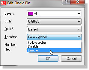
Note that the creation of a teardrop connection is dependant on the design rules. If making a teardrop connection would violate one of the design rules then it will simply not be created.
Configured teardrop connections will be made dynamically as we complete routes in the sections below.