Edit Room
Overview
A room definition is used to specify an area of the PCB for a particular task such as placement or design rules. This dialogue allows you to configure the room for a particular purpose. The two halves of the form are independent, so one room can serve as a placement room, as a design rule room, or as both.
Placement Room Options
Placement Mode
Select what components can be placed inside the room by the auto-placer.
- Ignore, not used by the auto-placer.
- Keepout, components are not placed inside the room.
- Any, any component can be placed inside the room.
- Group, components belonging to a particular placement group can be placed inside the room.
If you select Group then the Group combo box underneath is enabled, allowing you to specify which group you want to place in the area.
See Also:
Layer
Specify whether the placement room applies to the Top Side, the Bottom Side or All. This will determine where components are allowed to be placed; All hosts the group on both sides of the board.
Hide label
Check this box to suppress the room's label on the layout. There is one checkbox and it hides whichever label the room currently displays, that is the group name for a placement room and the room name for a design rule room.
Design Rule Room Options
Using Design Rule Rooms
First, a quick recap on how to use design rule rooms.
- Place the room, give it a name and a layer range.
- Go to the Design Rule Manager (Technology menu) and create one or more design rules that apply to the room.
- Review the design rules in the Design Rule Manager to confirm that your changes are correct. Select a region on the left hand side (the room, for example) and the right hand side will show you the design rule or rules that apply inside that region.
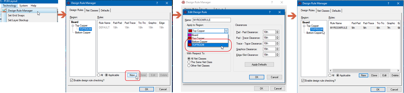
Creating a design rule scoped to a room in the Design Rule Manager
The following reference manual topics contain more information:
Design Rule Hierarchy (which rules have higher priority over other rules).
Name
Provide a name for the DRC room. This will appear in the Design Rule Manager dialogue so that you can apply design rules to the room.
From layer / To layer
Specify a start and stop layer for the room. In some cases (escaping a BGA, for example) setting a room to cover multiple layers is really useful. However, bear in mind that it might complicate the design rule hierarchy. Check the room entry on each layer carefully in the Design Rule Manager when you have created your rules.
Exclude Foreign
When checked, all copper within the room boundary that does not belong to the same object group as the room is flagged as a DRC violation. This effectively creates an exclusion zone on the room's copper layers. To use this feature, group the room with the component whose copper should be permitted inside the boundary.
Zone fills automatically punch a void matching the room boundary when this option is enabled. Traces that are electrically connected to a grouped component's pads (same subnet) are also exempt, even if the trace itself is not a direct member of the group.
See Also:
Via Style
Select a via style to override the net class default when vias are placed inside this room during interactive routing. This is useful for areas of the board where a different via type is required, such as a BGA escape area where micro-vias are needed.
If the selected via style is not compatible with the layer transition being made (e.g. a micro-via style is selected but the via spans more than one dielectric layer), the override is not applied and the net class default via style is used instead. A one-shot warning is displayed on the status bar when this occurs.
Use Microvia
When checked, this option filters the Via Style dropdown to show only via styles that are flagged as micro-vias. This makes it easier to select the correct micro-via style without having to scroll through all available via styles.
The checkbox is disabled, and cleared, in either of two cases. The first is a board without micro-via capability, that is one whose stackup has no micro-via drill span; the tooltip then reads "Requires a 1+n+1 HDI board stackup with microvia drill spans". The second, and the more common in practice, is a board that has the stackup but where no via style has been flagged as a micro-via; the tooltip then reads "No microvia via styles are defined". In the second case the remedy is to create or flag a micro-via style first, after which the checkbox becomes available.
Apply Style
Converts existing routed vias inside the room to the room's nominated micro-via style. For each via, Proteus checks whether the connected trace layers correspond to a valid micro-via drill span. Compatible vias are converted; incompatible vias are left unchanged. This is especially useful after autorouting, where all vias are placed with standard CNC styles.
Pressing the button also commits the changes you have made on the dialogue form, since it saves the room properties before applying the style.
The via style override is not a design rule. It changes the default via used during routing but is not enforced by the DRC checker. For a detailed explanation including a worked example of how the layer range compatibility check operates, see the topic linked below.
See Also: