MEASURE AND MOVE EXAMPLES
Introduction
The examples below cover a range of common measurement and positioning tasks in PCB layout. Each example shows how to use Measure Mode and the Measure Panel to check distances and reposition objects. For general information on Measure Mode, measurement modes, and the Measure Panel, see the main Measure and Move topic.
Pre-Requisites
All examples assume that you have a board layout open in ARES and that the objects you want to measure are placed and visible. Where an example involves components, it is assumed that a netlist has been loaded and the components are on the board.
Entering Measure Mode
Each example begins with "Enter Measure Mode". To do this, select Measure Mode from the mode toolbar, below the 2D graphics modes. The normal object selector panel is replaced by the Measure Panel, and the cursor changes to snap to object edges and boundaries. You are now ready to click on objects to measure between them. For full details on the Measure Panel controls, snapping behaviour, and measurement modes, see Measure and Move.
Example: Fiducial to Board Edge
Board fiducials are typically placed a fixed distance from each nearby board edge (commonly 3 mm to 5 mm) for pick-and-place machine vision systems. This means two separate measurements are needed: one from the bottom edge and one from the left edge (for a bottom-left corner fiducial).
Measuring the Horizontal Distance (from the Left Edge)
1) Enter Measure Mode.
2) Left click on the left board edge. The cursor snaps to the edge of the board outline.
3) Left click on the fiducial pad. The cursor snaps to the pad edge.
4) In the Measure Panel, select Octo-linear Aligned Points. This constrains the measurement to a pure horizontal distance from the board edge to the nearest point on the fiducial pad, ignoring any vertical offset between your click points.
5) Read the Horizontal distance in the Measure Panel. If the fiducial is around 4.15 mm from the left edge and the specification requires 5 mm, proceed to move it.
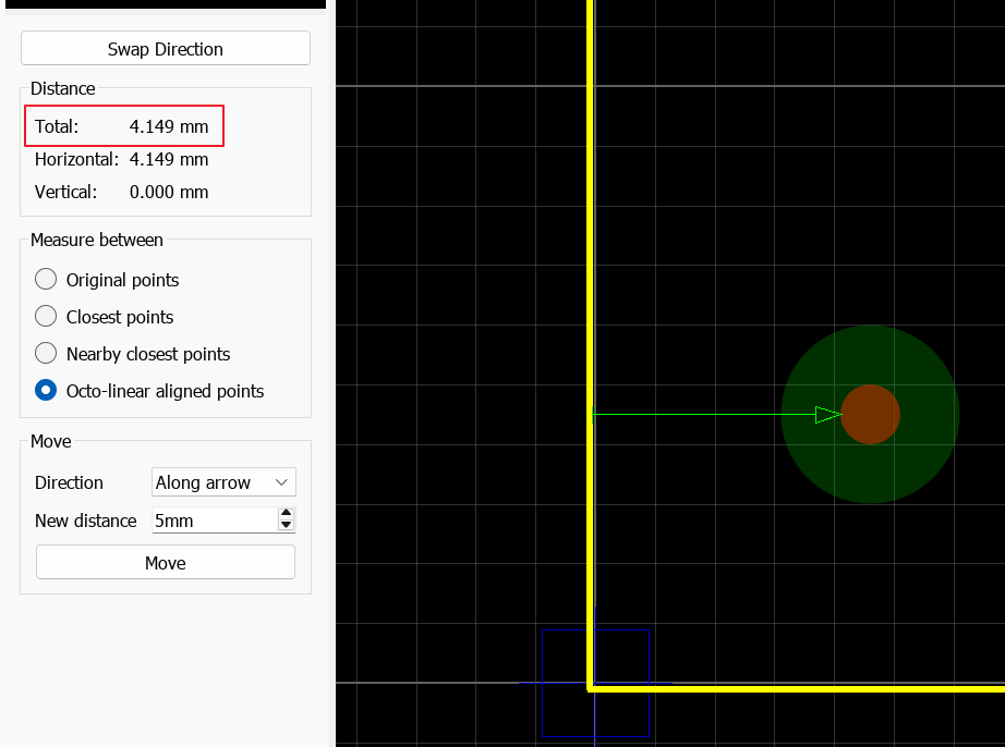
Reading the horizontal distance from the left board edge to the fiducial pad
Adjusting the Horizontal Distance
1) If the arrow points from the board edge to the fiducial, the fiducial is object B and will be the object that moves. If the arrow points the other way, click Swap Direction.
2) In the Move group, set Direction to Horizontally.
3) Change the New Distance value to 5 mm.
4) Click Move. The fiducial repositions so that its nearest edge is exactly 5 mm from the left board edge.
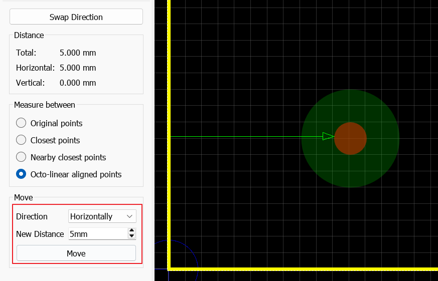
Measuring the horizontal distance from the left board edge to a fiducial pad using Octo-linear Aligned Points mode, then moving the fiducial to 5 mm.
Measuring and Adjusting the Vertical Distance (from the Bottom Edge)
1) With the fiducial now at the correct horizontal position, start a new measurement. Left click on the bottom board edge.
2) Left click on the fiducial pad again.
3) Select Octo-linear Aligned Points. This time the measurement constrains to a pure vertical distance.
4) If the vertical distance is not 5 mm, set Direction to Vertically, enter 5 mm, and click Move.
The fiducial is now exactly 5 mm from both the left and bottom board edges.
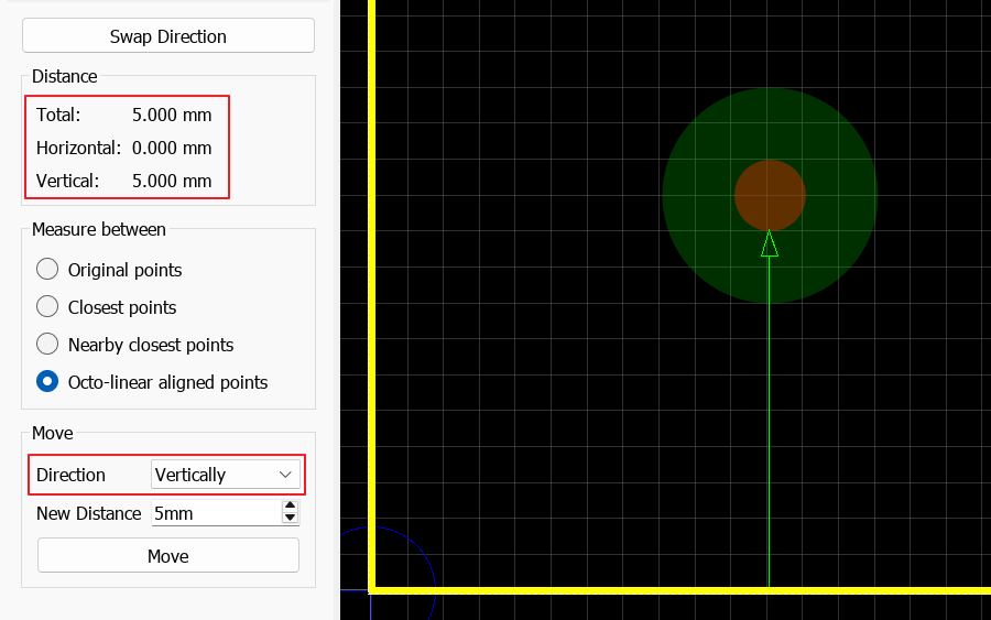
After both adjustments, the fiducial sits 5 mm in from the bottom edge and 5 mm in from the left edge.
If you have fiducials on multiple corners, measure and move each one independently. Alternatively, place the first fiducial precisely and use Replicate to create the others at known offsets from it.
Example: USB Connector to Board Edge
When a connector must protrude through a case wall, the distance from the connector body to the board edge is critical. Too far in and the connector does not reach the case aperture; too far out and it fouls the case wall. This is especially important for surface mount connectors like the USB MINI-8 SMT, where the connector face typically sits flush with or just inside the board edge.
In this example a USB MINI-8 SMT connector sits near a chamfered (45°) board edge. The enclosure drawing specifies 1.5 mm clearance between the connector body and the edge. Because the edge is diagonal, a simple horizontal or vertical measurement would overstate the true gap: what matters is the perpendicular distance from the edge to the connector body.
Measuring the Clearance
1) Enter Measure Mode.
2) Left click on the connector body (the courtyard or silkscreen edge, not a pad). When you are zoomed in on the connector area, this is the object you are most likely to click first.
3) Left click on the diagonal board edge segment near the connector. The cursor snaps to the edge of the board outline.
4) Select Nearby Closest Points. Because this mode finds the shortest distance between the two shapes in the area you clicked, it naturally returns the perpendicular distance from the connector body to the diagonal edge, which is exactly the clearance that matters for the case wall.
5) Read the distance. If it shows 2.3 mm and the specification requires 1.5 mm, the connector is too far from the edge and needs to move closer.
The measurement is correct regardless of which object you clicked first. The direction of the arrow does not affect the distance values in the Measure Panel.
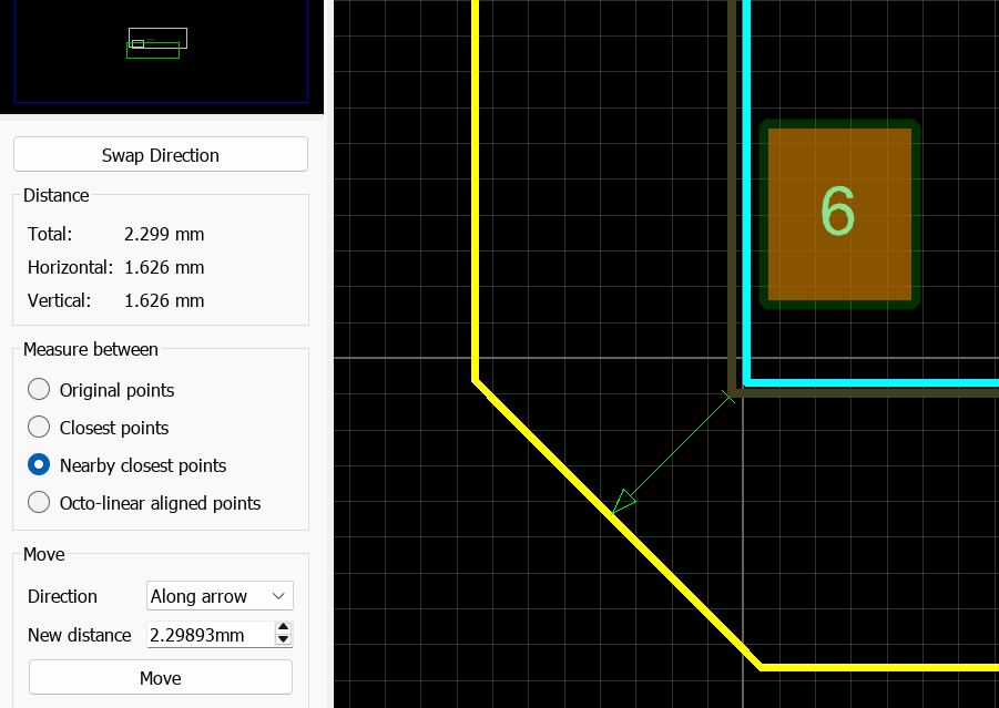
Nearby Closest Points measurement from the connector body to the diagonal board edge showing a perpendicular distance of 2.3 mm. The arrow tip is on the board edge.
Repositioning the Connector
Because you clicked the connector first and the board edge second, the arrow currently points from the connector to the board edge. The board edge is at the arrow tip (object B), meaning that clicking Move would reposition the entire board outline, which is almost certainly not what you want.
1) Click the Swap Direction button on the Measure Panel. The arrow reverses so that it now points from the board edge to the connector. The connector is now object B and will be the object that moves.
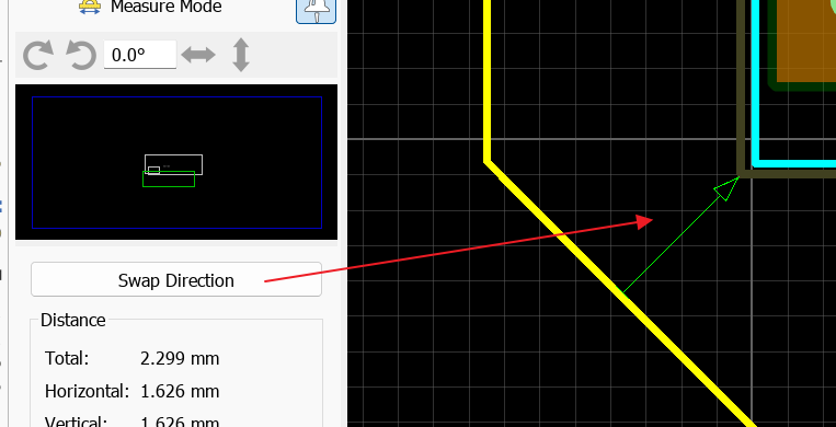
After clicking Swap Direction: the arrow now runs from the board edge to the connector body. The connector is at the arrow tip and is the object that will move.
2) Set Direction to Along Arrow. This moves the connector along the perpendicular to the diagonal edge, which is the direction that changes the clearance most directly. Using Horizontally or Vertically here would move the connector along one axis only, which for a 45° edge would change the gap by only 0.71× the movement distance.
3) Enter 1.5 mm in the New Distance spin box.
4) Click Move. The connector repositions so that the perpendicular clearance to the diagonal edge is exactly 1.5 mm.
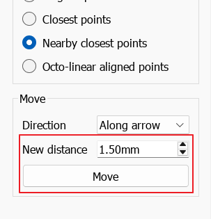
After the move: the connector body is now 1.5 mm from the diagonal board edge.
For a connector on a straight (horizontal or vertical) board edge, the same workflow applies but you can use Horizontally or Vertically as the move direction, since the perpendicular coincides with a single axis. Nearby Closest Points still gives the correct edge-to-edge distance.
Always check the arrow direction before clicking Move. The object at the arrow tip is the one that moves. If the arrow points towards a board edge, a zone, or another large object, clicking Move will reposition that entire object. Use Swap Direction to ensure the smaller, intended object is at the tip.
Example: Mounting Hole Spacing for an Enclosure
You are designing a board to fit an existing enclosure whose datasheet specifies four M3 mounting holes on an 100 mm × 65 mm rectangle. The bottom-left hole is the datum, positioned 5 mm in from the left board edge and 5 mm up from the bottom edge. The remaining holes are at (85, 5), (5, 55), and (85, 55) mm relative to the board corner, that is spaced 80 mm horizontally and 50 mm vertically from the datum hole.
The datum hole is already placed correctly (verified using the same technique as the fiducial example above). You now need to check that the bottom-right hole is exactly 80 mm to the right of it.
Checking the Horizontal Spacing
1) Enter Measure Mode.
2) Left click on the datum hole pad (bottom-left). The cursor snaps to the pad centre.
3) Left click on the bottom-right hole pad.
4) Select Original Points mode. Since both clicks snapped to pad centres, the distance shown is the centre-to-centre spacing, which is what the enclosure drawing specifies.
5) Check the Horizontal component in the Measure Panel. If it reads 79.5 mm instead of 80 mm, the hole needs to move 0.5 mm to the right.
Correcting the Position
1) Ensure the arrow points from the datum hole to the bottom-right hole (Swap Direction if needed). The bottom-right hole is object B and will be the one that moves.
2) Set Direction to Horizontally. This ensures the hole moves only along the X axis, preserving its vertical position.
3) Enter 80 mm in the New Distance spin box.
4) Click Move. The bottom-right hole repositions so that its centre is exactly 80 mm from the datum hole centre.
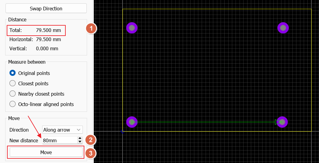
Measuring the centre-to-centre horizontal distance between the datum mounting hole and the bottom-right hole using Original Points mode, then moving the hole to 80 mm.
Verifying the Vertical Spacing
Repeat the process for the top-left hole: measure from the datum hole, select Original Points, check the Vertical component reads 50 mm, and correct if needed. The top-right hole can then be verified against both the top-left (80 mm horizontal) and the bottom-right (50 mm vertical) to confirm the full rectangle.
If a mounting hole is part of a component footprint (for example, a connector with integral mounting pegs), it cannot be moved independently, since the entire component moves. In that case, position the component first using its functional pads, then verify that the mounting holes land at acceptable positions relative to the enclosure specification.
Example: Component Body Clearance
Tall components such as electrolytic capacitors, transformers, or relays need sufficient clearance between their bodies for rework access, airflow, or to prevent physical interference. A typical requirement is 2 mm between capacitor cans.
Checking the Gap
1) Enter Measure Mode.
2) Left click on the body (courtyard or silkscreen edge) of the first capacitor.
3) Left click on the body of the second capacitor.
4) Select Closest Points. The arrow repositions to show the absolute minimum gap between the two component shapes.
5) If the distance is less than your required clearance (e.g. 2 mm), proceed to move one component.
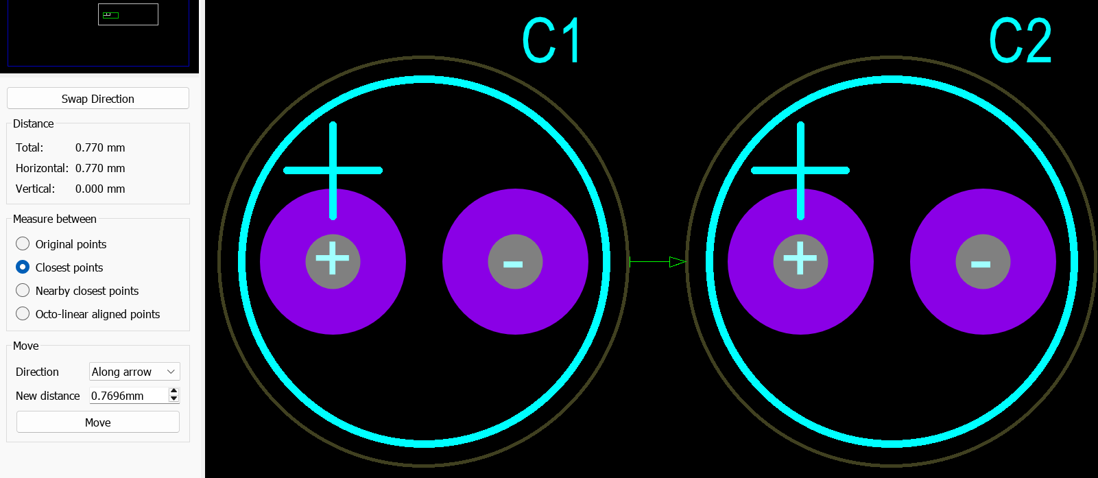
Closest Points measurement between two electrolytic capacitor courtyards, showing the minimum physical gap.
Adjusting the Gap
1) Check which component is at the arrow tip (object B). Swap Direction if you want to move the other one.
2) Set Direction to Along Arrow (to push the component directly away), or Horizontally/Vertically if you want to constrain the movement to one axis.
3) Enter 2 mm (or your required clearance) in the New Distance spin box.
4) Click Move.
5) Verify the result: the Measure Panel updates automatically with the new distance.
After adjusting component spacing, check that nearby silkscreen text is not obscured by the moved component. You can use a second measurement between the component body and the silkscreen line to verify this.
Example: Heatsink and Mechanical Part Clearance
Heatsinks, battery holders, and other mechanical parts often need clearance for clips, cables, or insertion access. The courtyard or silkscreen outline of the footprint represents the physical extent of the part.
1) Enter Measure Mode.
2) Left click on the edge of the heatsink footprint (courtyard or silkscreen).
3) Left click on the nearest neighbouring object (component body, board edge, or connector).
4) Select Nearby Closest Points to get the edge-to-edge gap in the area you are interested in.
5) Check whether the gap is sufficient for the spring clip or cable that needs to pass through. If a clip is 3 mm wide and needs 1 mm clearance either side, you need at least 5 mm total gap.
6) If the gap is insufficient, enter the required distance and click Move to reposition the neighbouring object.
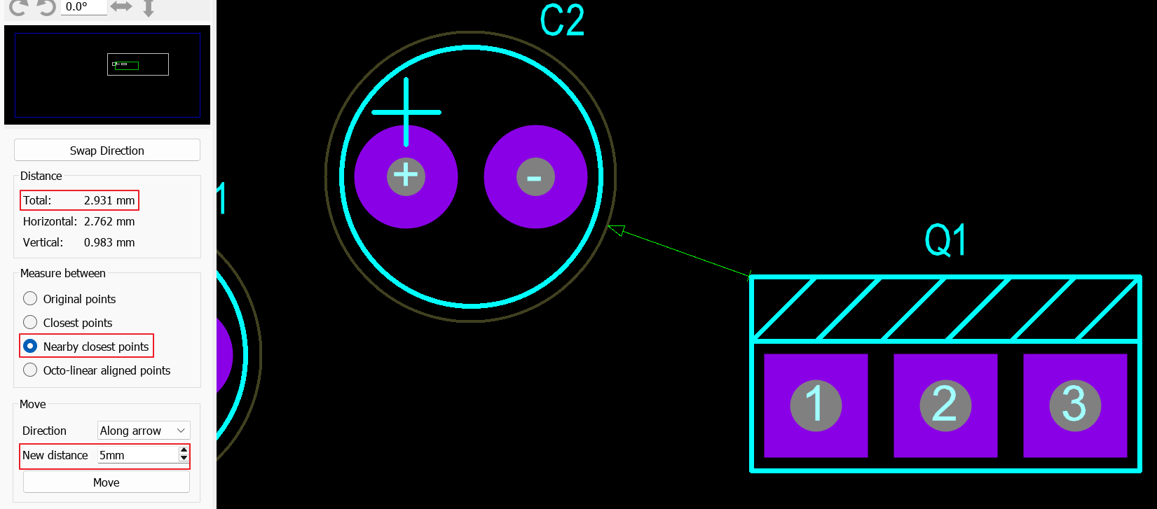
Measuring the edge-to-edge clearance between a heatsink footprint and a neighbouring component using Nearby Closest Points mode.
Example: Testpoint Spacing for Probe Access
In-circuit test fixtures require testpoints to be spaced far enough apart for pogo pins or spring probes. Typical requirements are at least 2.54 mm (100 mil) centre-to-centre, with 1.27 mm (50 mil) as an absolute minimum.
Checking Centre-to-Centre Spacing
1) Enter Measure Mode.
2) Left click on the pad centre of the first testpoint.
3) Left click on the pad centre of the second testpoint.
4) Select Original Points. The distance shown is the pad-centre to pad-centre spacing.
5) Compare with the probe specification.
Checking Pad Edge Clearance
If the probe specification defines clearance as an edge-to-edge gap rather than a centre-to-centre pitch:
1) Make the same measurement as above.
2) Switch to Closest Points. The arrow repositions to show the minimum gap between the pad edges (copper to copper).
3) Compare this value with the probe clearance requirement.
Adjusting Testpoint Position
1) If the spacing is too tight, choose the appropriate direction (Horizontally or Vertically, depending on the testpoint arrangement).
2) Enter the required spacing in the New Distance spin box.
3) Click Move to reposition the second testpoint.
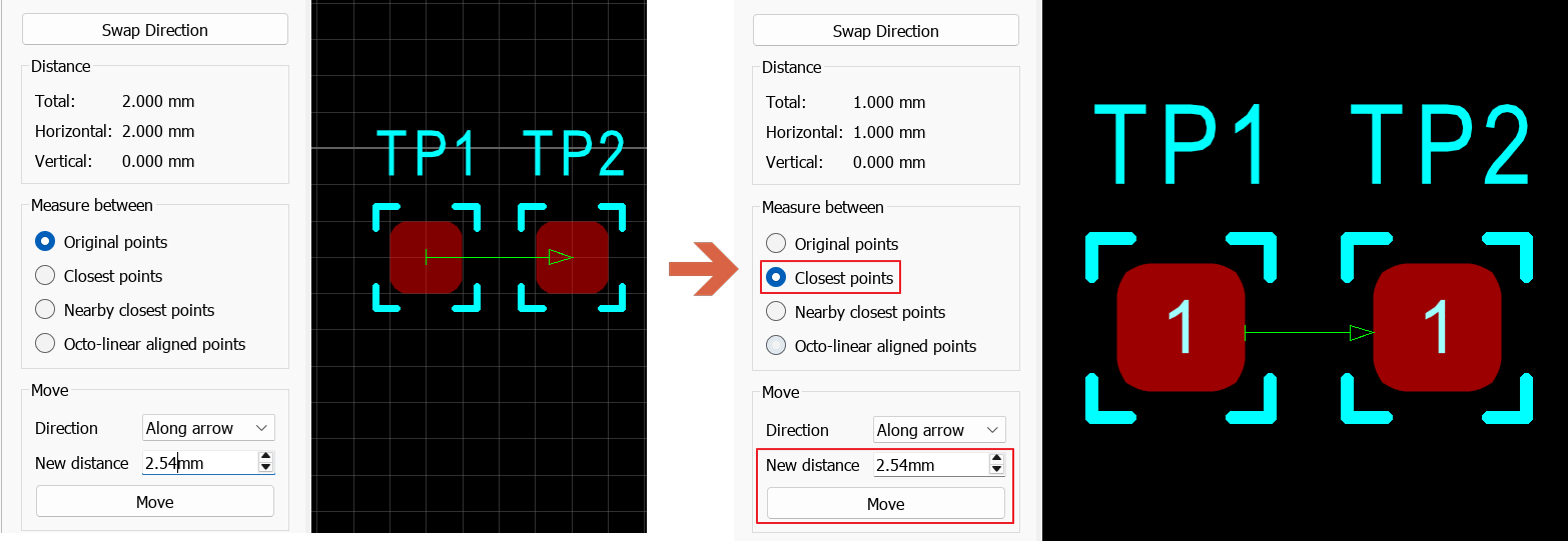
Measuring testpoint pad-centre to pad-centre spacing, then switching to Closest Points to check the pad-edge to pad-edge gap.
After adjusting individual testpoints, verify that the moved testpoint has not introduced a DRC violation with nearby traces or pads.
Example: Silkscreen Line to Pad Edge
Silkscreen lines and text should maintain a minimum clearance from copper features to prevent soldermask issues during manufacture. A typical clearance is 0.15 mm to 0.3 mm from pad edges.
1) Enter Measure Mode.
2) Left click on the pad edge you want to measure from.
3) Left click on the silkscreen line or text.
4) Select Closest Points to find the minimum gap between the copper pad and the silkscreen feature.
5) If the gap is too small or too large, ensure the arrow points towards the silkscreen object (Swap Direction if needed), enter the desired clearance in New Distance, and click Move.
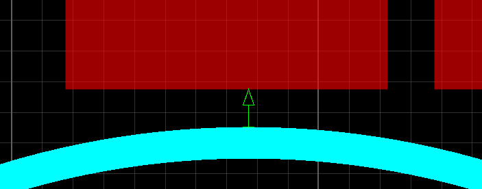
Measuring the minimum gap between a pad edge and a silkscreen line using Closest Points mode.
Example: LEDs in a Case Aperture
Four status LEDs (D1 to D4, using LEDC1608X60 footprints) must sit inside a rectangular window in the enclosure front panel. The enclosure drawing specifies the aperture as 20 mm × 3 mm, positioned with its bottom-left corner 12 mm from the left board edge and 8 mm from the bottom board edge. Each LED body is 1.6 mm × 0.8 mm.
This example covers the full workflow: drawing the aperture outline on a mechanical layer, positioning it relative to the board corner, placing the first LED inside the aperture with Measure and Move, then using Replicate to place the remaining three at a defined separation.
Pre-Requisites
Before starting, ensure D1 through D4 are placed on the board (from the netlist) and that the schematic references are in order. Replicate uses reference increment to bind replicated copies to schematic parts, so D1, D2, D3, D4 must exist as sequential references in the schematic.
Step 1: Draw the Aperture Outline
1) Select the 2D Graphics Box mode from the left toolbar.
2) In the layer selector, choose a mechanical layer (e.g. Mechanical 1). Do not use the Board Edge or Slot layers: this is a reference outline only, not a board feature.
3) Draw a rectangle 20 mm wide × 3 mm tall at an approximate position. The exact location does not matter yet.
Step 2: Position the Aperture Relative to the Board Corner
The aperture must be 12 mm from the left board edge and 8 mm from the bottom edge (measuring from the bottom-left corner of the aperture to the respective board edges).
1) Enter Measure Mode.
2) Left click on the left board edge.
3) Left click on the left edge of the aperture rectangle.
4) Select Octo-linear Aligned Points to get the pure horizontal distance.
5) Ensure the arrow points from the board edge to the aperture rectangle (Swap Direction if needed). Set Direction to Horizontally, enter 12 mm, and click Move.
6) Now measure the vertical position: left click on the bottom board edge, then left click on the bottom edge of the aperture rectangle.
7) Select Octo-linear Aligned Points, set Direction to Vertically, enter 8 mm, and click Move.
The aperture outline is now correctly positioned with its bottom-left corner at (12, 8) mm from the board corner.
Step 3: Position D1 Inside the Aperture
1) In Measure Mode, left click on the left edge of the aperture rectangle.
2) Left click precisely on the left edge of D1's courtyard outline. Zoom in and click the courtyard boundary line itself, not the copper body fill and not the component label area.
3) Select Octo-linear Aligned Points. This constrains the measurement to a pure horizontal distance, ensuring the snap runs cleanly along the X axis from the aperture edge to the courtyard edge.
4) Ensure the arrow points towards D1 (Swap Direction if needed). Set Direction to Horizontally, enter 2 mm, and click Move.
5) Now centre D1 vertically. Left click on the centre line of the bottom edge of the aperture rectangle, then left click on the occupancy cross (centre marker) of D1. Select Octo-linear Aligned Points, set Direction to Vertically, enter 1.5 mm, and click Move.
The 1.5 mm value is simply half the aperture height, which places D1 on the centre line of the aperture. Measuring to the centre line of the aperture outline rather than to its inner or outer edge keeps the figure independent of the line width of the graphics style you drew the rectangle with.
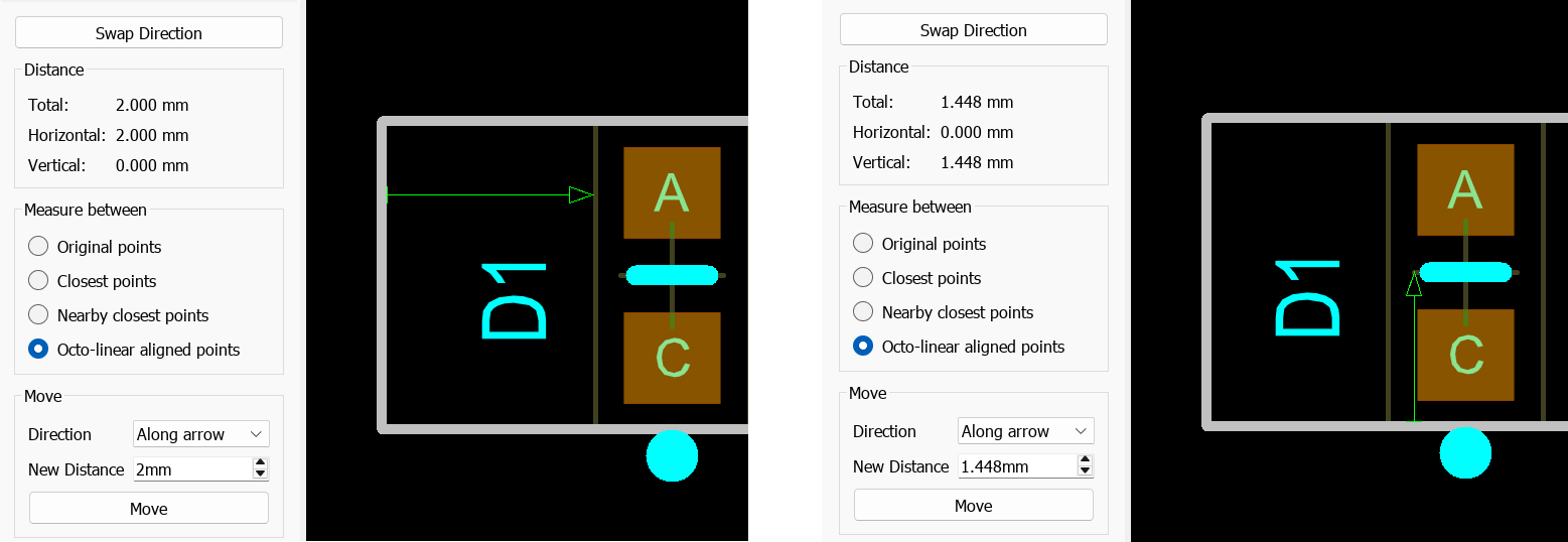
D1 positioned 2 mm from the left edge of the aperture outline and centred vertically within it.
Step 4: Replicate D2, D3, D4
The remaining three LEDs need to be spaced evenly to the right of D1 with a 3 mm edge-to-edge gap between the LED bodies. With 1.6 mm body widths and 3 mm gaps, the four LEDs span: (4 × 1.6) + (3 × 3) = 15.4 mm, leaving a 2 mm left margin and a 2.6 mm right margin within the 20 mm aperture.
1) Exit Measure Mode. Select D1 and choose Replicate from the right click context menu (or Edit Menu).
2) Set No. of Copies to 3.
3) Choose Separate (not Offset). This defines the spacing as the gap between physical edges rather than as a centre-to-centre pitch.
4) Set X-Step to 3 mm and Y-Step to 0 mm.
5) Set Relative to to Object Extremity or Courtyard, so that the separation is measured between the physical boundaries of the LED footprints.
6) In the Re-Annotation group, set Bind To to D2 and Increment to 1, so that the copies bind to D2, D3 and D4 from the schematic.
7) Click OK. Three copies appear to the right of D1, each with a 3 mm gap between the LED bodies.
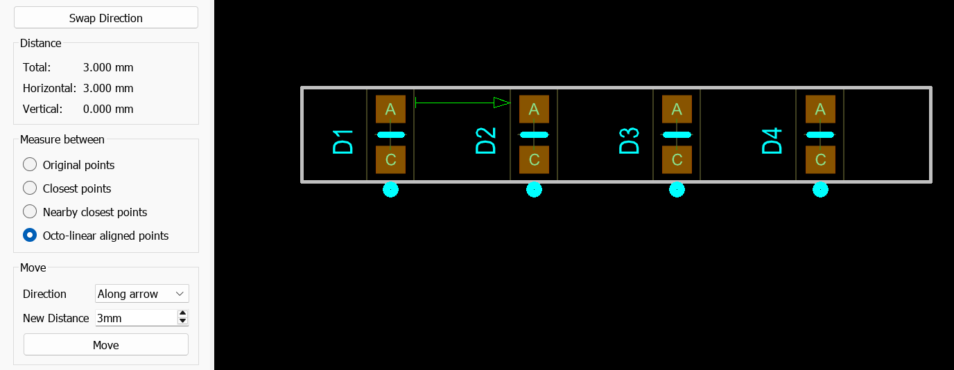
Four LEDs (D1 to D4) replicated at 3 mm edge-to-edge separation inside the aperture outline on the mechanical layer.
Step 5: Verify
1) Enter Measure Mode and spot-check the gap between D1 and D2. Left click on D1, then D2, and select Closest Points. The distance should read 3 mm.
2) Check the gap between D4 and the right edge of the aperture. Left click on D4, then the right aperture edge, and select Nearby Closest Points. This should read approximately 2.7 mm, confirming that the LEDs sit symmetrically within the aperture.
Replicate in Separate mode produces edge-to-edge gaps that are directly equivalent to the distances Measure Mode reports with Closest Points or Nearby Closest Points. This makes the two tools a natural pair: use Measure and Move to position the first object precisely, then Replicate to produce the remaining copies at the verified separation.
Example: Assessing Routing Space Between Objects
Before committing to a routing strategy, it is useful to know how much space is available between two objects for traces to pass through.
1) Enter Measure Mode.
2) Left click on the edge of the first object (pad, via, or component body).
3) Left click on the edge of the second object on the other side of the intended routing channel.
4) Select Closest Points to find the minimum gap.
5) Compare this gap with the width required for your traces. For example, if you need to route two 0.2 mm traces with 0.15 mm clearance either side and between them, you need at least (2 x 0.2) + (3 x 0.15) = 0.85 mm of gap.
If the gap is insufficient, consider moving one of the objects using the Move function, switching to a narrower trace style, or finding an alternative route.
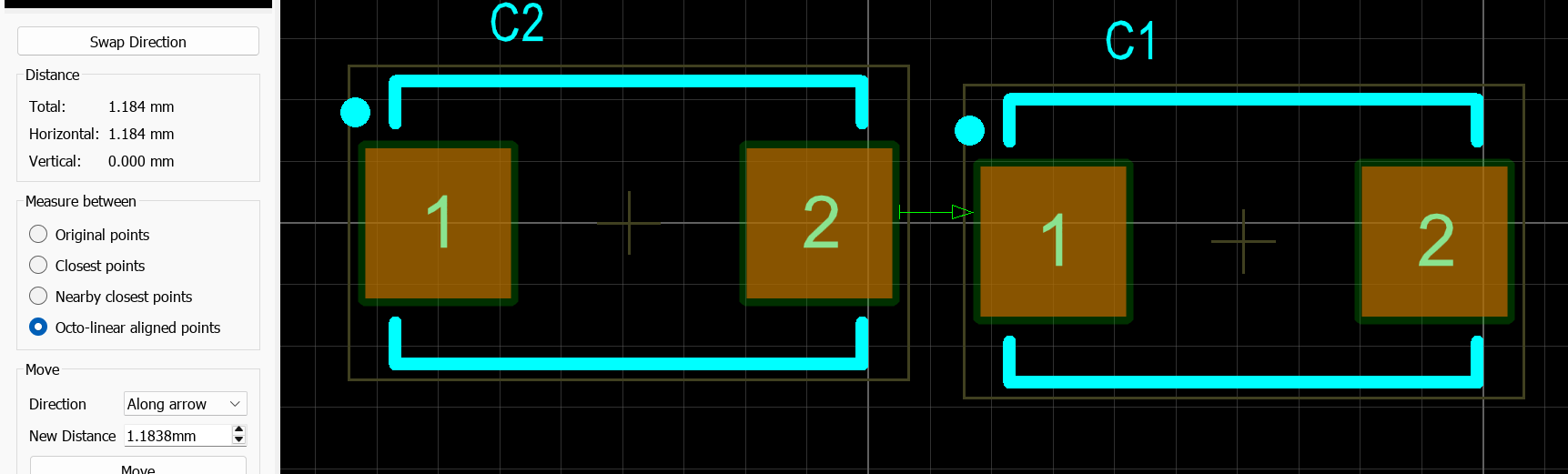
Measuring the available routing channel between two pads using Closest Points mode, showing the edge-to-edge gap.
Example: Checking Silkscreen Visibility Between Components
Component reference designators and other silkscreen text can be obscured when components are placed close together. Use Measure Mode to check and adjust the gap.
1) Enter Measure Mode.
2) Left click on the silkscreen text of the component reference (e.g. R1).
3) Left click on the body of the adjacent component.
4) Select Closest Points to find the minimum gap between the text and the component body.
5) If the text is too close (or overlapping, shown as a zero or negative effective distance), reposition the text label or move the component to create adequate clearance.
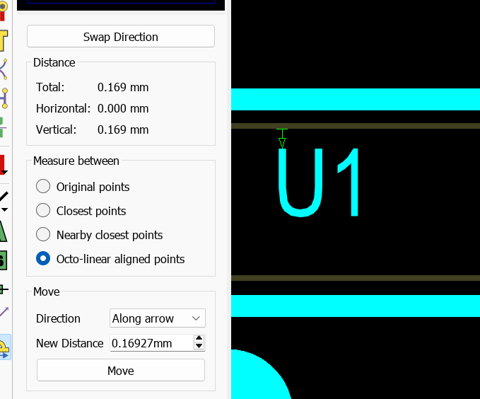
Checking the gap between a reference designator and the neighbouring component body
Remember that silkscreen text can be repositioned independently of its parent component by dragging on the label. You do not always need to move the entire component.
Example: Offsetting a Header by its Own Pad Pitch
This example demonstrates the Move By behaviour, which applies when both ends of the measurement arrow land on the same object. The Move group offsets the entire object by the entered amount, rather than repositioning it relative to a second object.
Two CONN-SIL3 headers (J1 and J2, both with the SIL-100 footprint and 0.1 inch / 2.54 mm pad pitch) are placed on the board for a daughterboard connection. J2 is correctly placed, but J1 has been positioned one pitch too far to the left, so its pad 1 sits directly above where pad 2 should be and the two connectors are offset by exactly one pin position. Rather than calculating the offset or aligning by eye, the pad pitch of J1 itself is the value to move by, and Measure Mode can read it off the component directly.
Measuring the Pad Pitch
1) Enter Measure Mode.
2) Left click on the centre of pad 1 of J1 (the misaligned header).
3) Left click on the centre of pad 2 of J1, the adjacent pad on the same component.
4) Select Original Points mode. The Distance group shows the centre-to-centre pitch: Total 2.54 mm, Horizontal 2.54 mm, Vertical 0.000 mm.
All four Measure Between modes remain available here. The two click points are on the same component, but they snapped to two different pads, and Closest Points is only disabled when both ends of the arrow land on the same feature. Original Points is the mode this example uses, since the pitch is a centre-to-centre dimension.
Offsetting the Header
Because the arrow connects two points on the same object, the Move group displays Move By instead of New Distance. The Move function will now offset the entire J1 header by the amount entered, rather than positioning it relative to anything else.
1) Set Direction to Horizontally. (Vertically and Along arrow are also available; Horizontally matches the axis of the misalignment.)
2) In the Move By spin box, enter 2.54 mm. A positive value shifts J1 in the direction of the arrow (left to right, since the arrow runs from pad 1 to pad 2). If the arrow ran the other way, you would enter -2.54 mm or click Swap Direction first.
3) Click Move. J1 is offset by exactly one pad pitch to the right. Its pad 1 now occupies the position formerly held by pad 2, and the two headers are correctly aligned with pad 1 of J1 in line with pad 1 of J2, and so on.
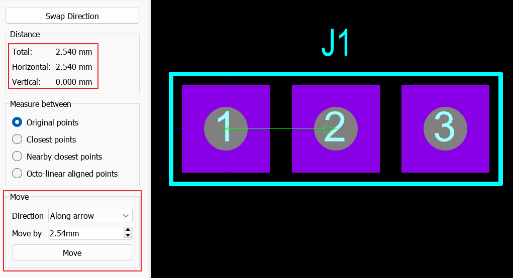
J1 offset by exactly one pad pitch so that it lines up with J2
Move By is useful any time you want to shift an object by a measured dimension you can read off the object itself: pad pitch on a connector or BGA (to step a part by one or more pin positions), the body width of a chip to step it one footprint sideways, the length of a trace segment to extend a related feature by the same amount. Combine with Replicate when you need many copies at the measured spacing.
Move By offsets the whole object as a rigid body. It does not change the dimension you measured. To change the pad pitch within a footprint you must edit or replace the footprint; Measure Mode cannot alter internal geometry.
See Also: