IDF OUTPUT
Overview
The Intermediate Data Format (IDF) is a specification designed to exchange printed circuit assembly (PCA) data between mechanical design and PCB layout. Initially developed in 1992, the IDF format has since become a de facto industry standard.
The format includes all information that is commonly shared among mechanical design, circuit board layout and physical analysis and is directly supported by most MCAD products including Solidworks, although it has now largely been superseded by the STEP/IGES file formats.
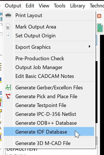
Export in this format with the Generate IDF Database command on the Output Menu. This opens the IDF Manufacturing Output dialogue, which has two tabs: IDF Output holds the settings, and Log reports the result of the generation.
Exporting in the IDF format
To generate an IDF fileset for the layout
- Select the Generate IDF Database command from the Output Menu in the layout.
- Specify the Filestem and Folder for the output. Both fields accept field codes.
- Choose whether to write individual TXT files or a single ZIP archive, and whether Proteus should open the output folder or the ZIP file automatically when it has finished.
- Select the layers to be included in the output. This will default to the layers used in the current project.
- If the layout contains bitmaps or true-type fonts, set the rasteriser Resolution. The choices are 125, 250, 500 and 1000 dpi.
- If you want a common solder resist expansion (guard gap) across the entire layout then check Apply Global Guard Gap and set the clearance.
- Click Generate to produce the IDF fileset, then read the Log tab to confirm that it completed cleanly.
Slot data does not need to be identified. Any cut-out drawn on the Slot layer, and any slotted padstack, is picked up automatically. See Mechanical Routing & Slots for the detail.
Note that IDF output is fundamentally a 2D format that contains some 3D information. This information is taken from the 3D Visualisation parameters such as height specified for the footprint (right click on package, select make package and switch to the 3D tab). If no 3D information is supplied a default is passed.
The board and feature thickness is taken from the Set Board Properties command on the Technology menu.
See Also: