TESTPOINTS
Introduction
Testpoints can be used on the PCB in many different ways, ranging from sporadic coverage for calibration and monitoring where it's deemed necessary to more rigorous coverage for bed of nails or flying probe testing. Proteus allows you to work with testpoints in the way which best suits your design. You can simply place and designate testpoints as needed or set up a testpoint coverage strategy and the work to ensure compliance.
Creating Testpoints
A testpoint can be either a dedicated pad or it can be an existing pad/via already on the layout. Where it is a dedicated pad the process starts on the schematic with the placement of a testpoint terminal.
Placing a Testpoint Terminal
To place a testpoint terminal:
- Select terminal mode on the schematic and the testpoint terminal.
- Left click to start placement and use the + and - keys on the numeric keypad to rotate the terminal.
- Left click again to drop the terminal.
- Wire up in the normal way.
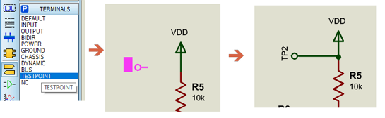
Placing a Testpoint Terminal on the Schematic
For each testpoint terminal there is a testpoint package on the layout. This must be also placed and connected up

Testpoint Pad needs placing and connecting on the layout.
Important: all testpoints placed this way will be packaged with the same package. You can change the default package (Design Rule Manager > Defaults tab, Default package for testpoint terminals) but it applies to all testpoint terminals. If you need different pad sizes you can use the designate method below.
Designating a Testpoint on the Layout
To designate a testpoint on the layout:
- Enter selection mode
- Right click on the pad or via
- Select testpoint from the context menu.
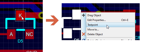
Specify a pad as a testpoint from the context menu.
You can only create a testpoint where the pad size is larger than the specified minimum dimension of pad shape. This is set on the Design Rule Manager > Defaults tab and is intended to ensure that a probe can always connect. The access side and the minimum separation between test points are enforced at the same moment; see Testpoint Rules and Clearances.
Whether you choose to work with testpoint terminals on the schematic, designate testpoints on the layout or work with a mix or both probably depends on board density, required coverage (and maybe corporate policy).
Using testpoint terminals on the schematic has some advantages :
- They are visible on the schematic.
- They are automatically and uniquely annotated (e.g. TP1, TP2, etc.)
- They're obvious and easily located on the board.
There are also however some disadvantages:
- Each terminal requires the placement of a new pad on the layout. Often the designation of an existing pad is more convenient and saves space.
- If you want large scale testpoint coverage it's a lot of terminals to place on the schematic.
- Each testpoint based on a schematic terminal will (must!) have the same footprint.
Testpoint Rules and Clearances
The Testpoints group on the Defaults tab of the Design Rule Manager holds six settings, all of them global to the board. Three of them govern where a testpoint may be placed or designated and are described here; the coverage settings are described under Testpoint Coverage below, and the default package is described above.
All three placement rules are enforced at the moment you designate a testpoint, not merely reported afterwards. If the pad is too small, if it is on the wrong side for the access setting, or if it is closer to an existing testpoint than the minimum separation, the designation is refused and a message appears on the status bar.
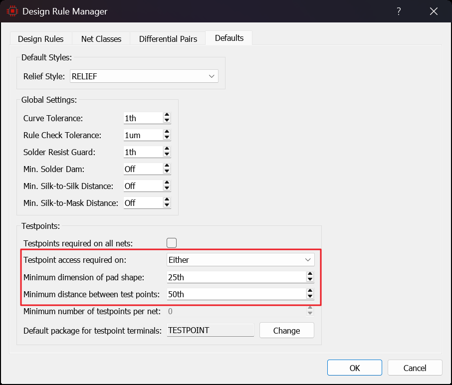
Testpoint placement and clearance settings.
Testpoint access required on
Determines whether testpoints must be on a particular side of the board, bottom for a bed of nails for example, or whether access is possible from either side. The three values are Either, Top and Bottom.
Minimum dimension of pad shape
Determines the minimum size of pad shape required for the testpoints. This is required of all dimensions of the pad (e.g. length and width for rectangular pads). To comply with the test land guidance in the testability provisions of IPC-2221, set this to at least 0.9 mm (35 thou).
Minimum distance between test points
This distance is governed by the pitch limitations of ICT probes and so should be set in consultation with testing to ensure access. A value of 2.54 mm (100 thou) suits standard ICT probe pitches.
These constraints are designed to cover the basics and help with a successful testpoint strategy. They do not however guarantee a successful test point strategy. For example, no consideration is made of placement inside component bodies (rendering the testpoint inaccessible after assembly, component heights (which can obstruct access for probes) or pin length which can determine whether sufficient exposed pad is available for probes on designated testpoint pads.
Testpoint Coverage
If you decide to use testpoints formally in your project then ensuring adequate coverage is important. This could be as simple as making sure there are at least two testpoints per net for flying probes or it could be something like ensuring that each power net has testpoints (or both).
There are two ways to specify coverage, both of which take place in Design Rule Manager.
Global Coverage
Specify that testpoints are required on all nets and also the minimum number required per net.
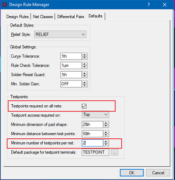
Set global testpoints requirements.
Net Class Coverage
You can override the global settings per net class. Depending on what you need this allows you either:
- Have no requirement for testpoints on all nets and simply set the testpoint requirements on the net class(es) you are interested in.
- Set a global requirement for testpoints on all nets and then override for specific net class(es). Here for example you might set to zero for a net class not requiring testpoints or 3 for a net class requiring more testpoints.
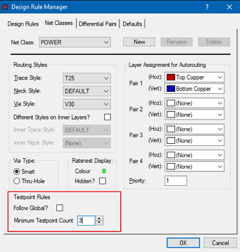
Override any global coverage settings for the current net class.
If you choose to set testpoint requirements (and you don't need to) then both placed and designated testpoints will contribute to the required total for the net.
Testpoint Compliance Workflow
So, now you've set up your testpoint strategy and it turns out there's a couple dozen nets needing at least 2 testpoints each. The system now needs to help you:
- See what testpoints are specified on the board.
- Tells you which nets are compliant and which are not.
- Helps you work through the nets to achieve compliance.
In Proteus we do this using the Testpoints filter on the net list in connectivity highlight mode.
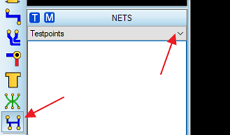
Testpoint Viewing Mode.
Depending on your configuration what you're likely to see here initially is a mass of red non compliant nets! Each net will show the required number of testpoints for that net (if any specification has been made) or just the number of testpoints placed if not.
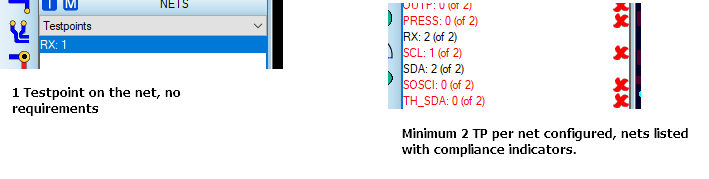
If you set up minimum requirements then the testpoint filter will show you which nets need attention.
If you double click on a net in the net list two things will happen. First the net will be selected entirely, including all pads and tracks. Second, any existing testpoints will be tagged in yellow so you can see them.
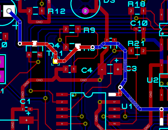
Net highlight with the existing placed testpoint tagged yellow.
For arguments sake lets assume we want to designate a second pad to be a testpoint (rather than place one). All we need do is right click on a pad or via and select the Testpoint command from the context menu.
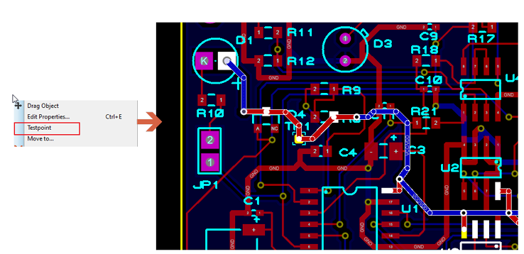
Second pad designated as testpoint on the net.
The net list at this point will update and the net will show as compliant since it is has the minimum required number of testpoints. We can continue by double clicking on the next non compliant net to tag it.
In summary, if you have set up minimum requirements for nets the workflow to make sure you have sufficient coverage is :
- Enter testpoint filter view via connectivity highlights.
- Tag the first non compliant net by double clicking on it.
- Right click on pads and select testpoint to designate them or place and connect the TP footprint if you are working with schematic terminals.
- When the net has the right number of testpoints move on to the next one.
Reporting and Output
It's important to understand that the Testpoints filter on the net list checks only that the right number of testpoints are placed or designated. If the rest of the net is unrouted for example that's a separate problem which will be highlighted by missing connections in the CRC report. There are several additional reports and output files which can be generated.
Designated testpoints also flow into the IPC-D-356 netlist that is included with every Gerber X2 CADCAM output. Supplying that netlist satisfies the CAD data requirement of IPC-9252 (section 5.1.2), the standard governing electrical test of unpopulated boards.
Pre-Production Check
This is the most rigorous report, generated by the Pre-Production Check command on the Output menu in the layout module, as it checks the board in general as well as the testpoints. In our example above the pre-production check would fail with a connectivity error if the net was not properly routed.
The results of the pre-production check can also be inserted into a Project Notes report as a data table, alongside the testpoint reports described below.
See Also:
Testpoint Reports
Project Notes provides two testpoint report templates, and between them they cover the three items below:
- Testpoints, a data object containing the location of each testpoint on the board, together with a graphic showing where each one sits.
- Net Testpoint Count, a data object containing the compliance status of each net against the specified constraints, with columns Net, Specified and Actual. This is the compliance artefact that the whole Testpoint Coverage section builds towards.
You can modify the information in either report as needed. PDF output can be generated directly in the Project Notes module.
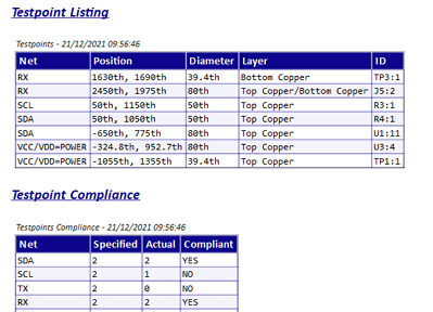
Example of location and compliance data objects in the testpoint report.
Gerber X2
Gerber X2 files identify testpoints using the TESTPAD attribute. This is included with the Proteus output for all specified testpoints. Note however that testpoints designated on component pads will instead have the COMPONENTPAD attribute as this is documented as higher priority in the specification.
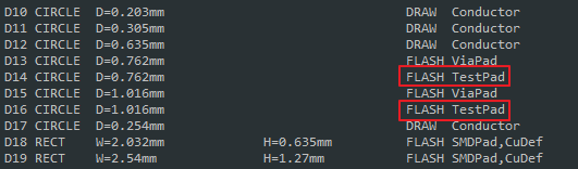
The TESTPAD attribute written into a Gerber X2 file
Testpoint Information File
The Generate Testpoint File command on the Output menu writes a .TPI file. It is comma delimited but carries a descriptive text header, so it is not a plain CSV. Each testpoint is written with six fields:
- ID, the reference of the testpoint.
- Type, either THRU for a through-hole pad or SURF for a surface pad.
- X and Y, the centre of the drill hole or the pad origin relative to the Output Origin, in the units currently set for the layout.
- Net, the net the testpoint belongs to.
- Layer, one of TOP, BOTTOM or TOP/BOTTOM.
Vias are only listed if they are exposed through the solder resist.
Print Mode
You can print a testpoint plot using the testpoint mode on the print dialogue form, with the option of including the appropriate silk and copper layers as well.
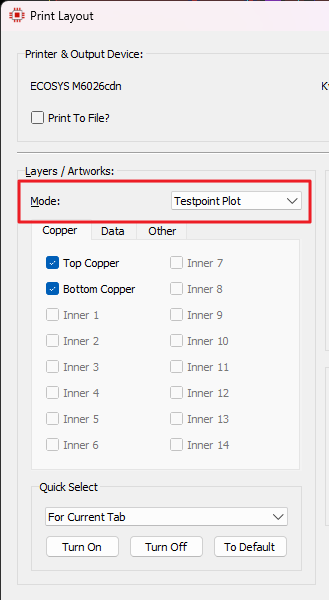
The testpoint print mode on the print dialogue
See Also: