PRE-PRODUCTION CHECKLIST
Overview
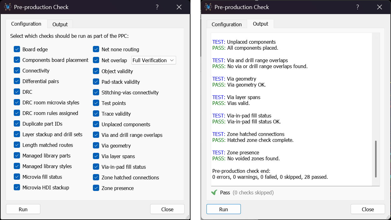
PPC Tabs.
The pre-production checklist is an automatic test of your layout for common errors which is normally launched prior to sending the board for manufacture. It can also be launched manually with the Pre-Production Check command on the Output Menu. We strongly recommend that you resolve any errors that are reported in this check before production of any hardware. Running the checklist and archiving its report in the manufacturing pack also provides the design review evidence recommended by the design for excellence guidelines of IPC-2231.
You can disable specific checks for the current session by turning off the appropriate checkbox before running the checklist. This should be done with caution.
The pre-production check is an aid to and not a replacement for manual inspection of the layout and designer approval. Quality assurance responsibilities lie with the board designer. In particular, Labcenter always recommend the creation and testing of a physical prototype prior to mass production.
You can copy the results of the Pre-Production Check to the clipboard using keyboard shortcuts (CTRL+A to select all and then CTRL+C to copy to clipboard).
If you run the Pre-Production Checker (PPC), then close it and make some modifications to the board, next time you open the PPC it will display an Out of Date message to let you know that the PPC has not been run since modifications were made:
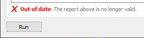
The out of date message shown when the board has been modified since the last check.
Reporting the Results
When Gerber files are produced following a PPC run the results of the PPC are stored in the readme.txt file, including any fails or warnings.
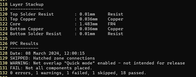
The pre-production check results written into the CADCAM readme file.
The results can also be placed into your documentation. Insert a Pre-Production Check data object into a note in the Project Notes module and the check log appears as a formal table of results, followed by a summary counting the errors, warnings, failures, skipped checks and passes. This is the tidiest way to ship evidence that the board was checked alongside the manufacturing pack.
The data object reports the results of the last run. If the checker has not been run, or the board has changed since, run the Pre-Production Check first and then regenerate the object.
The Checks
The following is a list of the checks performed and the suggested course of action when errors are reported. They are listed in the order the dialogue lists them.
Board edge
This checks that the board edge is present and complete (no gaps). If this fails you should either place a board edge or rework the existing board edge so that it is complete.
Complex board edges are most often imported as DXF files. However, if created in Proteus they should always be drawn with the 2D Graphics Path tool as this guarantees a complete board edge. Curved segments can be drawn by holding down the CTRL key while placing the segment and the outline can be adjusted after placement via the drag handles. A right click context menu allows for the addition of corner vertices and bezier nodes after placement. Please see the section on the board edge in the tutorial for more information.
Components board placement
This checks that components are all inside the board edge and not placed outside and then forgotten about.
Fixing this error involves re-working the layout such that all components are inside the board edge.
Connectivity
This test automatically runs the CRC, and identifies whether all connections specified in the netlist have been made.
If this fails, you should launch the Connectivity Checker and double click on entries to locate and then track the missing connections on the layout.
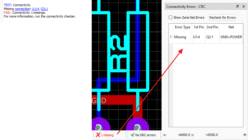
The connectivity report listing the missing connections on the layout.
Differential pairs
This checks for unrouted differential pairs and then checks whether routed diff pairs violate the max paired or max separation distances.
An error is also produced if the differential pair is deemed indecipherable (for example multiple routes, or extra pads connected).
You can use connectivity highlights mode filtered to diff pairs to quickly locate them on the layout.
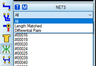
Filtering connectivity highlights to differential pairs.
The diff pair in question should then be inspected and corrected to be compliant.
A more rigorous report on Diff Pairs can be generated from Project Notes. This can be helpful in spotting errors.
DRC
This test re-runs the Design Rule Checker on the layout.
If the Design Rule Checker is disabled you should enable it from the Design Rule Manager on the Technology Menu.
If you have Design Rule Errors they can be viewed by clicking on the DRC Error report on the status bar at the bottom of the application. Errors can be located by double clicking the mouse on the resulting dialogue form.
Design rules are configured via the Design Rule Manager on the Technology Menu.
You should resolve all DRC errors before moving to manufacture. This may involve setting appropriate design rules for your layout (if you have not already done so), adjusting the layout to conform with the specified design rules or, very rarely, acknowledging the error as an intentional design decision and suppressing it by right clicking and selecting Ignore this Error from the resulting context menu.
DRC room microvia styles
Where a DRC room has micro-via mode enabled, this check verifies that the via style the room nominates is actually a micro-via style. A mismatch usually means the room was set up for HDI but its style was never converted, so vias placed inside it are standard vias.
This check only ever raises a warning; it does not fail. The Apply Style button on a DRC room can correct style mismatches in bulk.
DRC room rules assigned
This checks that all design rule rooms have a rule associated and that all rules which point to a room point to an existing room (that is, the room has not been deleted). You can locate and edit a room easily from the object selector while in Room mode.
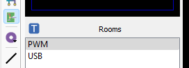
Locating a design rule room from the object selector in Room mode.
Duplicate part IDs
Checks that no two parts have the same silkscreen identifier or part reference. If you get this error you should find the two or more parts with the same reference (using Search & Tag, the T keyboard shortcut) and then change them such that the part references are all unique. You can do this with the Automatic Annotator (Tools Menu) either globally or just for the selected items.
Layer stackup and drill sets
This checks whether a valid layer stack has been defined for the current board. If none has, the check fails and reports that DRC results may be invalid, because many of the other checks depend on knowing the stackup.
Many modern output formats make use of the layer stack, and it allows the designer to specify more precisely the way in which they would like their PCB to be constructed. If a layer stack has not been specified you should define one with the Set Layer Stackup command on the Technology Menu.
See Also:
Length matched routes
This checks that tracks which have previously been length matched have not since been nudged or had their length changed.
When tracks are length matched they are considered internally to be part of a matchgroup. The target length (length of the longest track) and the tolerance (from the length matching dialogue) are stored after a successful length matching operation. This information is then retrieved by the PPC and the target length plus tolerance is tested against the real length of each of the tracks in their current state.
This also checks that differential pairs are compliant in terms of length and tolerances defined on the differential pair dialogue form.
The Length Matching report is a good place to review, audit or print the length match data used in your project.
Managed library parts
When the project is using managed library mode, this check verifies that all library parts in the design are managed. It flags any unmanaged devices or packages and any parts whose managed property values have been locally edited and are inconsistent with the library.
If this fails, review the flagged parts and either replace them with the managed library version or update the managed library to include them.
This check is skipped when the project is not using managed library mode.
Managed library styles
When the project is using managed library mode, this check verifies that pad style properties on placed components match the managed library versions. Differences can arise when a pad style is edited locally without updating the managed library.
If this fails, review the flagged components and synchronise the pad styles with the managed library.
This check is skipped when the project is not using managed library mode.
Microvia fill status
Micro-vias are normally required to be filled so that a subsequent layer can be built on top of them. This check counts every plated through micro-via that is not marked as filled and reports them as a warning; it does not fail.
To correct it, edit the via style and mark it as filled, or use the Via Inspector to locate and bulk-edit the micro-vias concerned.
Microvia HDI stackup
This checks that micro-via styles are only used on a board whose stackup actually offers micro-via drill spans. If micro-vias are present but the stackup has no such spans, a warning is raised suggesting that you either use an HDI stackup template or convert the micro-vias to standard vias.
The check is skipped where the board has no valid stackup at all, since there is then nothing to compare against.
Net none routing
This warns on the presence of routing with no net assigned, for example a loose trace. These can be dangerous because they are often unplanned (not represented on the schematic) and should be investigated.
Net overlap
This test goes through the layers one by one, imaging each net thereon and checking that no two nets overlap. Crucially, this tests all the power planes on the layout for overlap. This test should never fail. If a fail is reported please contact Labcenter support without changing the layout.
Selecting Full Verification mode (the default) uses a completely separate algorithm from the zone placement code in general use and therefore forms a secondary verification on zone integrity. Quick Check mode will use the much faster algorithm in the editor and therefore is less time consuming but also less rigorous, as a bug may be duplicated.
Always use Full Verification mode before any generation of production files.
This test can take some time, several minutes on a large board with many zones.
Object validity
This check tests the integrity of the layout objects and should always pass.
If this fails you should contact Labcenter support.
Pad-stack validity
This checks for instantiations of pad stacks which have no layers defined. This falls into the category of that which should not happen and can be fixed by editing the padstack style. Contact Labcenter support for assistance if needed.
Stitching-vias connectivity
This checks that stitching vias are still connected to two zones. It is possible through routing or object placement to change the area of a flood fill which could orphan a stitching via.
If you get an error here you need to either remove the stitching via or adjust the plane fill such that the location of the via is filled.
This check will only look at stitching and shielding vias placed automatically. It does not check vias placed manually.
Test points
The testpoint check ensures:
- The testpoints are bigger than the minimum specified size.
- That you have specified one of top, bottom or either for the testpoint location.
- That the testpoints are on the specified layer.
- That the testpoints are connected.
- That the testpoints are spaced apart further than the set minimum.
- If testpoints are required on all nets, that each net has at least the required number of testpoints.
See Also:
Trace validity
Performs a series of checks on the board tracking. It warns if tracking is found on unused or plane layers, and errors if zero length segments are found or if a segment's co-ordinates are too large.
Unplaced components
This simply checks that all the components specified in the netlist have been placed on the board. If it fails you need to place the components, or change the schematic and re-netlist if they are superfluous.
Via and drill range overlaps
This checks that via drill ranges used do not cause problems with manufacture of the board. Typically, this happens when you use both blind-top and blind-bottom vias and the drill ranges overlap. It also flags overlapping vias whose holes are not concentric, and overlapping vias of the same centre but differing hole diameters.
If you get an error here you need to either change the drill ranges to make the board manufacturable with standard processes or speak to your fab house to check if they can produce the board in its current form.
Via overlaps just means that the normal way of drilling then sandwiching boards is not going to work. It does not necessarily mean this is wrong if you and your manufacturer agree, for example on laser drilling.
Via geometry
This check inspects the physical proportions of every via on the board and covers three separate things.
Hole size
IPC-2226 defines a micro-via as a laser-drilled hole of 6 thou (0.15 mm) or less. A via style flagged as a micro-via but carrying a larger hole is not laser-drilled micro-via territory, so it is reported as a warning and is then held to the standard annular ring below rather than the more lenient micro-via one.
Aspect ratio
The aspect ratio of a micro-via is the drilled depth divided by the hole diameter, and it governs whether the plating chemistry can reliably reach the bottom of the hole. A ratio above 0.75:1 is reported as a warning, because IPC-2226 recommends that laser-drilled micro-vias stay at or below 0.75:1. A ratio above 2:1 is reported as a failure. The depth is taken from the layer stackup, so a board with no valid stackup is not ratio checked.
Annular ring
The annular ring is the copper remaining around the hole once it is drilled, and this part of the check applies to every via, not just micro-vias. The worst ring across the copper layers is compared against a minimum of 2 thou for a genuine micro-via and 3 thou for any other via, including an oversized micro-via as described above. A ring below the minimum is a warning. A negative ring, where the hole is actually wider than the pad, is a failure.
To correct any of these, edit the offending via styles, or review the layer stackup to ensure that micro-via spans are correctly defined. The Via Inspector can be used to locate and bulk-edit micro-vias.
The Microvia Compliance data object in Project Notes gives a per-via table of the aspect ratio, drill span and filled status, which is the right thing to put in a manufacturing pack. It does not test hole size, annular ring or DRC room style consistency, which are checked only here, so run the checklist as well as generating the report.
Via layer spans
This checks that valid and contiguous via ranges have been specified for the vias on the layout.
If you get an error here you need to edit your via styles and check the layer ranges.
Via-in-pad fill status
A via placed inside a surface mount pad must be filled, or solder will wick down the hole during reflow and starve the joint. IPC-4761 Type VII describes the filled and capped construction that prevents this.
This check counts vias that sit inside an SMD pad and are not marked as filled, and reports them as a warning. Only vias that break the surface on the top or bottom copper are examined, so the inner spans of a stacked HDI structure are not flagged here.
To correct it, edit the via style and mark it as filled, or move the via out of the pad.
Zone hatched connections
This checks that connecting pads are not smaller than the gaps in the hatching. If they are you get a warning and are advised to manually inspect or change pad sizes, because a poor connection is quite likely.
The hatching location is fixed, so if visual inspection shows that the hatch does intersect with the pad as intended then it will be safe. Decreasing the hatch spacing (via the edit zone dialogue) or increasing the annular ring size of the pad (via the pad style dialogue) will guarantee a connection between the two.
Zone presence
This checks the zones on every layer of the board, not just the copper layers, and reports two different conditions at two different severities.
A zone on a layer that does not exist in the layer stackup is a failure. If you see this, check the layer stackup configuration.
A zone with no copper in it, that is a voided zone, is only a warning. It usually means that routing or object placement has consumed all the available area within the zone boundary. Use the Zone Inspector to understand why the zone was voided and consider adjusting the zone boundary or removing conflicting objects.