DESIGN RULES
Introduction
Proteus PCB Layout includes an in-built verification system for testing and warning you when the clearance between objects on the layout is less than required for your design. This lies at the heart of the layout system and is the single most important set of information that you can provide to make the software work for you. It is therefore highly recommended that configuring and setting this up is one of the first things you do when laying out a new PCB; not only is it invaluable in avoiding errors but it is also harnessed by both the auto-routing and the manual routing engines to honour trace widths and clearance specifications.
Design rules work in levels of priority so that you can override one rule with another one in a granular way. You can narrow the scope of a design rule physically by reducing the area in which it applies to a single layer or an area of PCB called a design room. You can also narrow the scope of a design rule electrically by making it apply to a set of connections called a net class. Finally, you can mix the two together to create really granular rules that apply to a set of connections in a particular area of the PCB.
There is quite a lot to understand here so this page will start by introducing the key concepts before showing you how to set up clearances between object and design rules. You'll find quite a few links to more information on this page, much of which will also be required reading if you plan to design PCB's of any complexity
Key Concepts
This topic introduces the following key concepts that are required to correctly set up a constraint driven layout with Proteus:
- Net Classes
- Design Rooms
- Design Clearances
- Design Rules
- DRC Viewer
- Violation Areas
- Pairs
Net Classes
A net class is simply a net or group of nets that have common electrical characteristics (e.g. Mains Power). Once specified, you can control trace widths, via styles and layer sets for a net class as well as controlling clearances by creating net class specific design rules.
When you set the track width it will automatically be applied when routing a connection in the net class. So, for example, if the POWER net class was specified to have a 25th track you set it up here and then the software will select it for you when you are routing. If you have more than one supply and need different rules for each then just create another net class.
When you set the neck style you tell the software the minimum track width it can use to pass through dense areas. It also lets you take control during routing as holding the SHIFT key down will switch from track style to neck style.
Setting the via style has both economic and electrical consideration but, again, is worth setting up once and then letting the software do the work after that.
See Also:
Design Rooms
A design room is an area drawn out on the layout inside which specific clearances apply. Let's say for example that you have a BGA on your layout. This normally results in a routing challenge in escaping all of the tracks from the BGA where space is at a premium. To help with this you could draw a design room to encompass the BGA and the fanout area around it and then make the design clearances as small as possible in this fanout area. Design rooms can occupy multiple layers so that you could also via down and escape on inner layers.
More generally, you can think of a design room as the smallest physical area in which you can apply design rules. First, you can apply rules to the entire board, then you can apply rules to a single layer and then you can apply rules inside a room that you draw on the layer.
In addition to clearance rules, a design room can also specify a via style override to change the default via used during routing inside the room. This is particularly useful for HDI designs where micro-vias are needed in specific areas.
See Also:
Design Clearances
There are a number of physical design clearances that can be configured to provide real-time checking during the board layout. They fall into two groups. The first group is set inside each design rule, so the values can be varied by layer, by net class and by design room:
- Pad-Pad Clearance.
- Pad-Trace Clearance.
- Trace-Trace Clearance.
- Graphics-Net Clearance.
- Edge-Net Clearance.
The second group is global to the board. These clearances have no rule scope: one value applies everywhere, whatever design rules you have created. They are set on the Defaults tab of the Design Rule Manager and are covered under Global Clearances below:
- Solder Resist Guard.
- Min. Solder Dam.
- Min. Silk-to-Silk Distance.
- Min. Silk-to-Mask Distance.
Whilst the first three are largely self-explanatory, the definition of a pad for design rule purposes is worthy of mention. All pads, vias and padstacks that have an annular ring anywhere on any layer are considered pads. For example, a depleted via (non-functional pad) is considered a pad on all layers for design rule purposes. The clearance measurement starts at the hole border on depleted layers and at the edge of the annular ring on normal layers. Padstacks with no copper on inner layers are treated in exactly the same way.
The only pad like entities not treated as pads for design rule purposes are mounting holes. Here, you place a pad, edit it and set to be a mounting hole. This will remove the annular ring from all layers and the design rule that then applies is the edge/cutout clearance.
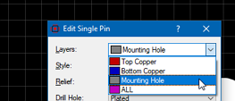
Mounting Holes are treated as Edge/Cutout for Design Rule purposes.
See Also:
If it's not a mounting hole, the pad->pad and pad->trace rules apply to all pads, vias and padstacks.
The other point of note is how design rules interact with power planes. All borders of power planes are drawn with a trace and so pad->trace and trace->trace rules define the distance that the power plane should step away from other copper objects. The power plane will do this automatically according to the clearance rules in force on various areas of the board.
See Also:
Graphics-Net clearance allows you to set the minimum clearance between a silkscreen graphic and any other object on the board. This is useful as the silkscreen graphic approximates the dimensions of the physical package.
Edge-Net clearance allows you to set the clearance between the edge of the board and any other object on the board. Note that this applies to interior edges as well (cutouts etc.). For different clearances around different edges you should set up the default rule for the main board edge and then use design rooms around the smaller cutouts to change the clearances in those areas.
Global Clearances
The four clearances in this section are global to the board. Each has a single value that applies everywhere, and each is set on the Defaults tab of the Design Rule Manager (Technology > Design Rule Manager). None of them can be varied per rule, per layer or per room.
Solder Resist Guard
The solder resist guard clearance is global to the board. This is a check for exposed copper features as a result of solder mask expansion around a pad. For example, if you edit a pad style to have a 10th guard gap (solder mask expansion) but you set your pad-trace design rule clearance to 6th then it is possible to end up with 4th of exposed copper trace should the trace hug the pad.
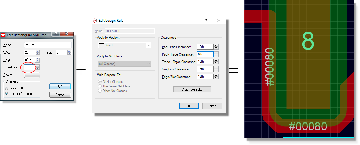
Often this is not a problem but, depending on the board topology, it can lead to solder bridges. It is generally good practise to have a pad-track design rule well in excess of the guard gap on the pads. This normally involves first checking with your board house on their recommended guard gap clearance and then adjusting pad style settings accordingly.
The Solder Resist Guard clearance defaults to 1th and will generate a DRC error wherever a copper object falls within 1th of the solder mask edge.
Minimum Solder Mask Dam
The minimum solder mask dam or the solder mask sliver refers to the size of the soldermask between pads. Having a solder mask dam can help prevent solder bridging during assembly. However, this depends on how the board is being constructed (e.g. reflow solder machine) and also with some fine pitch IC's the pins are so close together that there is no solder mask dam between pins.
For this reason the minimum solder mask dam is defaulted to OFF.
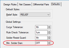
The minimum solder mask dam setting in the Design Rule Manager
If your design warrants a minimum solder mask then you can change it via Design Rule Manager and that value will be enforced. Be prepared to see a lot of violations initially - you will need to edit pad styles and change solder mask openings (guard gap size) on most IC's.
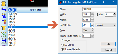
Changing the Guard Gap on a pad style before applying the change to the design.
Interesting fact (or urban myth?). Apparently, for the best solder mask dam you should make your PCB colour green. For example, if you choose 0.1mm for the dam then green would be 0.1mm, red,yellow,blue boards would need 0.12mm and black would be 0.15mm.
Silk-to-Silk
The control is Min. Silk-to-Silk Distance. This rule checks when two silkscreen objects on the same layer (Top or Bottom) are too close to each other. When enabled, you'll be warned if they fall within the specified clearance. Its primary purpose is to ensure silkscreen readability and avoid inks overlapping, which could lead to smudging or misinterpretation during assembly. This setting can be found on the Defaults tab of the Design Rule Manager and is set to Off by default.
Silk-to-Mask
The control is Min. Silk-to-Mask Distance. Again this setting can be found on the Defaults tab of the Design Rule Manager and is set to Off by default. This rule warns when silkscreen elements encroach on solder mask or paste mask areas. Enabling it protects pad openings: silkscreen ink over exposed copper or mask openings can impair solderability, interfere with component placement, or be clipped unpredictably during CAM. Although fabs often auto-clip such overlaps, fabricators may reject boards with silks on pads or mask openings.
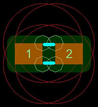
Silkscreen ink encroaching on a solder mask opening, reported by the Silk-to-Mask rule
8 mil (0.20 mm) is common; some sources accept 4 mil (0.10 mm) in tight designs. Check what your manufacturer is comfortable with.
These two rules are named after their controls on the Defaults tab, Min. Silk-to-Silk Distance and Min. Silk-to-Mask Distance. You may also see them referred to as silk-to-silk and silk-to-soldermask, which are the same two rules.
When you first turn this clearance rule on don't be surprised to see hundreds of Silk-to-Mask DRC errors, especially for parts such as 0805 resistors where silks are often drawn very close to pads. You should remake the part with smaller or more compliant silk graphics:
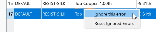
Ignoring a specific silkscreen DRC error from the right click menu in the DRC list
If you find yourself doing this a lot and/or you are a common user of the web import and wish to filter your libraries into an approved set consider using the managed libraries workflow. There's an initial investment of time in setup but it provides a version controlled (SVN/Git), auditable set of library parts for use that is well suited to design changes, engineering revisions.
Ignoring Specific Errors
Sometimes a violation is acceptable, such as a silkscreen reference that you wish to keep close to a pad. To suppress a specific error:
- Right click on the error in the DRC list.
- Select Ignore this error.
An ignored error stays in the list but is struck through and greyed out, and it no longer counts towards the violation total shown on the Design Rule Viewer. The rule itself is untouched, so nothing is disabled globally.
Ignore this error is a toggle, so selecting it a second time on the same error brings that error back. To clear every ignore in one go, right click in the DRC list and select Reset Ignored Errors. This is worth knowing after a bulk ignore of silkscreen violations: it is the only way back to a full error count.
Enabling Silk-to-Silk or Silk-to-Mask incurs a performance cost: the DRC system must evaluate every vertex of silkscreen elements (lines, reference text, component outlines, etc.). For dense boards, this may noticeably slow DRC checks. It might be best in this case to enable these rules only in final validation stages.
See Also:
Design Rules
Design Rules can be thought of as providing the scope in which the clearances apply. The default scope for the rule is the whole board and you can then narrow this physically to a layer on the board or an area of the board (a design room). You can also narrow the scope of a design room electrically by making it apply only to a particular net class. Finally, you can use both techniques to restrict the scope to particular signals in a particular area.
The system provides you with a simple interface and a default rule applying clearances to the entire board but the scheme is extendable as required given the complexity of your design.
See Also:
Design Rule Viewer
The Design Rule Viewer is a live display (located by default towards the bottom right of the layout module) that will monitor and display the number of violations of the current design rule and clearance set specified for the layout.

The Live Design Rules Checker
Clicking on the display will then launch a popup listing showing more detailed information, including the design rule in question, the layer, the violation type and the clearance information. If you click on an entry in the list, Proteus will highlight the associated design rule flag on the layout, and if you double click an entry, the layout will both highlight it and zoom to its location on the board.
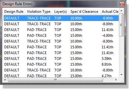
The Design Rule Checker form
The Design Rule Viewer will operate in the units specified for the layout (metric/imperial).
You can manually suppress any given error by right clicking on the error and selecting the ignore option. This is intended for the unlikely but not impossible case where a designer override is required.
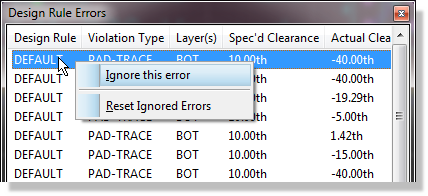
Suppressing a single violation with Ignore this error in the Design Rule Viewer
Violation Areas
When you click on an error in the design rule viewer the editing window will zoom around the offending area of the PCB and a highlighted violation area will appear. This area represents an area of violation of the rule specified in the Design Rule Viewer, and provides useful guidance as to what objects can be moved to fix the problem.
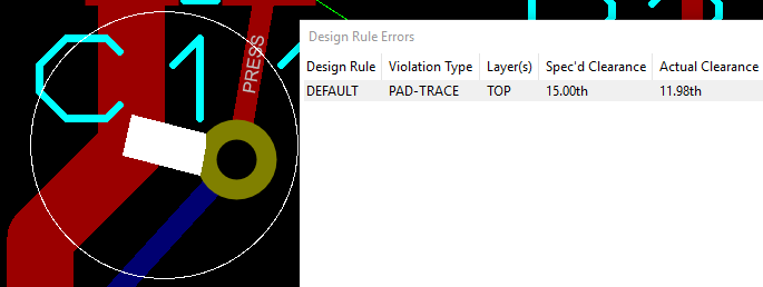
Violation Area showing the problem area between pad / via and trace.
Be aware that the violation area does not take account of whether the rule is actually in force over its entire area. For example, in the picture below the presence of the design room means that actually only the edges of the violation area (outside the room) are the cause of the design rule error. The trick is to first look at the rule that is being broken - since it is the default rule it should not apply in the room because any room rule would take precedence and therefore we should be looking outside the room boundaries to locate the actual infringement.
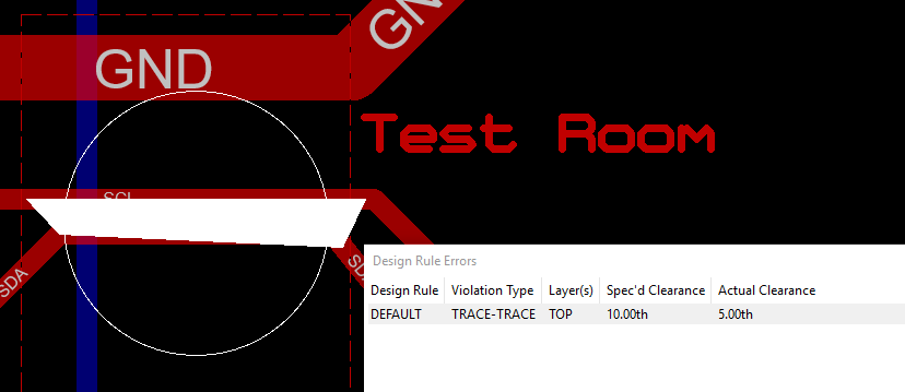
An example violation area which crosses a room boundary. The violation area shown is the area which breaks the currently selected rule. The presence of the design rule room here means in practice it is only the small area outside the room that is actually non-compliant with the rule set of the board.
Pairs
Pair information is used for differential pair routing and allows some more specific clearances to be included and stored. This information is specified on the diff pairs tab of design rule manager.
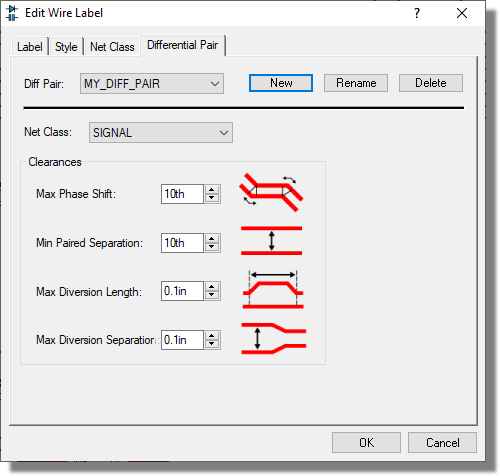
The Differential Pairs tab of the Design Rule Manager
See Also:
Setting Design Clearances
Design clearances can be set in two places; you can set the global default clearances or you can set clearances within a specific design rule.
The global design clearances apply to all signals on the board on all layers of the board and form the basis for the Default Design Rule; you can change these numbers, launch the Design Rule Manager from the Technology menu and set the rules under the DEFAULT Rule on the Design Rules tab.
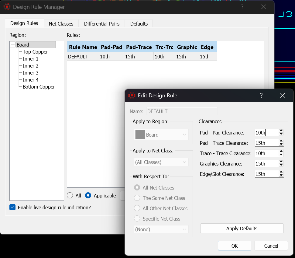
The Default Design Rules form
The Resist-Trace clearance is board global rather than per-rule. It is set on the Defaults tab of the Design Rule Manager as Solder Resist Guard.
Often it is the case however, where your design requires different clearances based on location (design rules per layer), based on electrical considerations (design rules per net class) or a combination of both. Proteus provides you with a method to specify any number of such design constraints via the Design Rule Manager command, located on the Technology menu.
To design to IPC-2221 (the generic standard on printed board design), take the electrical clearance for your operating voltage and conductor location from Table 6-1 of the standard and enter it as the clearance in a design rule for the affected net classes. The rule is then enforced during routing and verified by the design rule check.
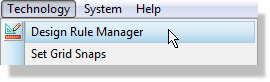
Launch the Design Rule Manager from the Technology menu
All such clearances are conditional and therefore form the basis of additional design rules. Put another way, you need to add a new design rule for each board requirement that differs from the manufacturing tolerances (the Default Design Rule). This is discussed in more detail in the next topic.
Design Clearances and Power Planes
For the purposes of design rules the border of a power plane is deemed to be a trace. The clearance between a power plane and a track is therefore the trace->trace clearance for the design rule currently being enforced and the clearance between a power plane and a pad/via is the pad->trace clearance of the design rule currently being enforced.
It's important to understand what this means. If you have a room on top copper and you have set clearances for both the room and the layer then a power plane on top copper will have different clearances to the pads and tracks depending on whether they are inside the room or not.
Should you need to have the same clearance everywhere on the power plane you can edit the zone and set the clearance field manually. As always with a duality the larger (safer) clearance will win. For example, a pad->trace design rule of 8th will be overridden by a zone dialogue clearance setting of 10th leaving the space between the pads and the zone at 10th. By contrast, if the clearance in the zone dialogue was set to 6th and the pad->trace design rule was 8th the clearance between the zone and the pad would be 8th.
A power plane will also step away from the edge of the board by the amount specified in the design rule manager for edge clearance. Since this value is rule specific and you can create single layer design rules it follows that you can define different edge clearances for power planes on different layers.
Setting Design Rules
Note: it's really important when you create a new design rule that you understand how the different types of rules will interact with each other. A rule with higher priority will have its clearances applied in precedence to a lower priority rule. This is explained in full in the topic on design rule hierarchy.
The Design Rules tab of the Design Rule Manager, showing the DEFAULT rule
The Design Rule Manager is the place where you can add additional rules specific to the current project. It has four tabs:
- Design Rules, where you create, rename, clone and delete design rules and edit the clearances they carry.
- Net Classes, where you define the net classes that rules can be scoped to.
- Differential Pairs, where you set the pair specific clearances described under Pairs above.
- Defaults, which holds the board-global settings: Solder Resist Guard, Min. Solder Dam, Min. Silk-to-Silk Distance, Min. Silk-to-Mask Distance, the tolerance settings and the testpoint settings.
Design Rules
This is where you create, rename and delete design rules or select an existing rule for editing. The Default rule is the global tolerance rule as discussed previously and is therefore permanent (cannot be deleted) and locked to all layers and all net classes.
Creating or editing an individual rule opens the Edit Design Rule dialogue. That dialogue is where a rule's scope and its clearances are set, and the sections below describe its fields.
Apply to Region
After creating a new rule you can specify the physical region the rule applies to. The choices are the whole board, a single layer, or a design room that you have drawn on the layout. This is how a room rule is created: draw the room first, then set Apply to Region to that room.
Apply to Net Class
When creating a new rule you can specify that a design rule applies to a specific net class or to all net classes from this selector. Note that the default rule is locked to all net classes and that only named net classes will appear in this selector.
For more information on defining net classes click here.
With Respect To
If you have defined a rule which applies to a specific net class you can then further refine the rule by specifying whether the rule applies only within the same net class, whether it applies only with respect to other net classes or whether it applies to both same net class objects and other net class objects.
Note that if you select either Same Net Class or Other Net Classes the graphics clearance and edge/slot clearance fields will be disabled as these objects are not specific to a net class and their meaning in such a case is ambiguous. These clearances are ignored for the purposes of such a rule.
Enable Design Rule Checking
This checkbox allows you to turn off the live checking for the currently selected rule. We recommend however that you leave this option selected.
Clearances
This is where you specify the required minimum clearances for the rule you are creating. The Apply Defaults button simply resets these clearances to those specified for the DEFAULT rule (Technology > Design Rule Manager, Design Rules tab).
The DEFAULT rule carries the board's manufacturing tolerances, so Apply Defaults returns the rule you are editing to those baseline figures.
Design Rule Reporting
You can generate report of all the design rules in force on the PCB via the Project Notes module. First, open Project notes and choose the design rule report from the template selector
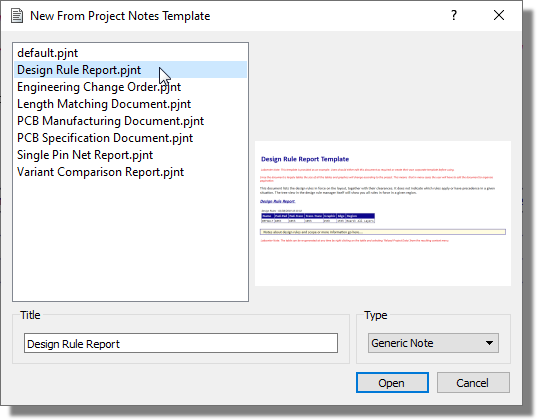
Choosing the design rule report from the template selector in Project Notes
If you already have more than one report open you can create the new report from the New Note command on the File Menu in Project Notes. The module needs to be unlocked to enable the new note command.
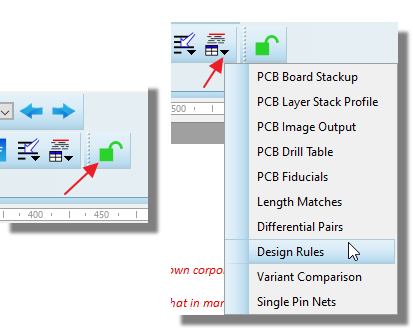
Inserting the design rule data into a new Project Notes note
The report will automatically generate and will list rules and clearances along with the layer ranges that they apply to. Note that the report does not include any concept of hierarchy but rather is just a complete listing of all rules set up for the current project.
If you do want to browse hierarchy and see which rules are in effect in a particular area of scope of the board the best place to do that is in the design rule manager itself. You can use the tree on the LHS to choose the scope you want and the right hand view will show you both the specified and inherited (grey in colour) rules that apply in your chosen scope.
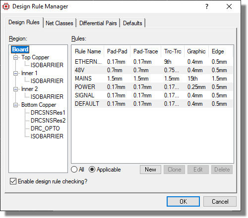
Browsing the rule hierarchy in the Design Rule Manager, with inherited rules shown in grey
See Also: