GROUND AND POWER RAILS
Why You Need a Ground
All simulations require a ground net to be defined. Without one, placing a probe on a particular net has no meaning, because the voltage on that net must be defined in terms of a fixed reference point. There is a further requirement that all parts of the circuit have a DC path to ground, since probing a point that is attached to a floating network is equally meaningless. Consider the circuit below.
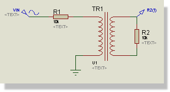
A transformer secondary with no connection to the ground reference
The secondary side has no connection to the ground reference, so the voltage at VB has no defined value. In theory we could have provided two pinned probes, as with a real multimeter, but there are serious mathematical difficulties in solving circuits without a ground, and Berkeley University did not address them in SPICE3F5. The simulator will supply a reference of its own in this situation, as described in the next section, but the value it then reports for VB is arbitrary. You should still ground the secondary yourself.
The ground net in a circuit can be defined either explicitly or implicitly. An explicit ground is defined by placing an unlabelled Ground terminal, as on the bottom end of RF2, above. You can also label a wire with the text GND if space is tight.
An implicit ground can be created through the use of a power rail, single pinned generator, loaded probe or a digital output, as well as by using any model that contains an internal grounded node.
Ensuring a DC Path to Ground
PROSPICE checks the DC paths in your circuit as the last step of building the simulation, after every object has been created. Interface objects and the power supply primitives generated for mixed mode circuits are therefore included in the check, which is why a design that looks floating on the schematic often is not.
Any analogue net that still has no DC path to ground is then repaired automatically. The simulator synthesises an earth resistor, connects it between the offending net and the ground net, and records what it did on the DC Paths diagnostic channel:
Added 100M resistor to ground for net VB.
The messages are informational rather than warnings, so you will only see them if you have switched the DC Paths channel on. The value of the resistor comes from the design property GEARTH, which is a conductance with a default of 1E-8 and therefore gives 100M ohms where a single net needs fixing. Lower the conductance for a higher value resistor.
The automatic repair keeps the simulation running, but a net that needed repairing was not the circuit you drew. Treat the DC Paths messages as a design review item rather than as noise.
Setting GEARTH=0 as a design property turns the repair off and restores strict behaviour. Each offending net then raises a warning on the same channel:
Net VB has no DC path to ground.
and the operating point solution will usually fail.
Another circuit configuration which has caused trouble in the past is shown below:
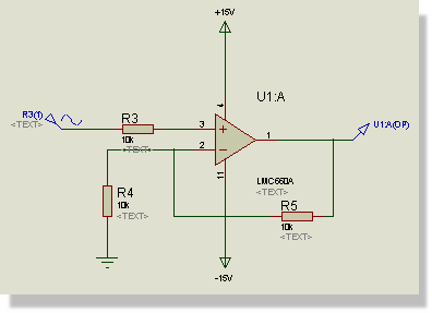
An output probe separated from the rest of the circuit by coupling capacitor C1
Here, the presence of coupling capacitor C1 means that the output probe has no DC path to ground, because the operating point is computed with all capacitors open circuit. The mechanism that resolves this is the simulator option RSHUNT, a resistance from every voltage node to ground with a default value of 1E12 ohms. It appears on the Tolerances tab of the simulator options dialogue as Shunt Resistance (Ohms), and it is written into every design whose options have ever been edited.
Capacitors can also be made slightly leaky individually, which is how the problem was solved before RSHUNT existed. Two properties control this, and either may be given on an individual capacitor or as a design property that applies to all of them:
- RLEAK, a leakage resistance in ohms. It takes precedence where both are given.
- GLEAK, a leakage admittance in Mhos.
A default GLEAK of 1E-12 is supplied automatically, but only to a design that carries neither an RSHUNT nor a GLEAK value of its own. Since almost every design carries RSHUNT, the capacitor leak is in practice something you set deliberately rather than something you inherit. Real capacitors generally have leakage considerably more than a million megohms, so the values involved are conservative, and the only circuits likely to notice are ones such as CMOS memory cells where charge is expected to be held for a long time.
Finally, a model author can declare which pins of a device conduct DC to which others by giving the part a DCPATH property. This overrides the path list built into the device type, and is the correct fix where the automatic repair is masking a model that does not describe its own conduction paths properly.
See Also:
Power
In general you should specify the power supply voltages for your simulations using the Power Rail Configuration dialogue form, which you reach from the Design menu of the schematic module.
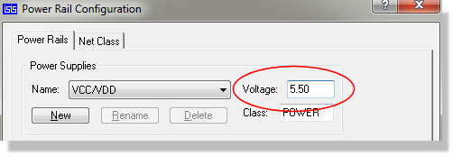
Voltage specified in the Power Rail Configuration dialogue form
There are essentially two stages to using this form:
- Create one or more power supplies as required using the &New button. Once you have created each supply, you can set its voltage in the Voltage: field. &Rename and &Delete act on the supply currently selected, and Class: sets the net class the supply's nets will be given in the PCB layout.
- Connect one or more power nets to each power supply by highlighting the names in the Unconnected power nets: list and then clicking &Add ->. The right hand list is captioned Nets connected to and the name of the supply, and <- &Remove puts a net back.
Note also:
- Power nets are created as a result of placing power terminals on the schematic and also when your design uses devices which have hidden power pins.
- You cannot simulate a design which has unconnected power nets. Attempting to do so will result in errors from the netlist compiler.
- You can also define power supplies on the schematic by placing power terminals with names of the form +5, -5 or +10V, -10V. The plus and minus symbols are crucial; a label such as 5.0V will not do.
- A default power rail configuration is provided which powers VCC/VDD at +5V, GND at 0V and VEE at -5V. VSS and GND are assumed to be interconnected. These defaults mean that most TTL, CMOS and microprocessor devices from the standard libraries can be simulated without the need to explicitly define any power supply connections.
- The Use default power rail connections? checkbox governs whether those defaults apply. Ticked, the shipped configuration is merged with whatever the design defines for itself; cleared, only the design's own rails and bindings are used. Either way the design's own definitions are held in the project as a PWRRAILS.DAT script, so a design with unusual supply naming keeps its configuration wherever it is opened.
See Also: