MIXED MODE INTERFACE MODELS (ITFMOD)
Overview
In designing our scheme for mixed mode simulation within PROSPICE, we gave considerable thought to the problem of how to specify the analogue characteristics of a digital device family. These characteristics include:
- The input and output impedances of the devices.
- The logic thresholds of device inputs.
- The voltage levels for high and low outputs.
- The rise and fall times of device outputs.
- The default logic state for floating inputs.
A scheme which involved specifying all these parameters for every device in the TTL libraries, say, would be extremely unwieldy.
A second problem arises in the specification of power supplies. It is natural to draw a circuit such as the one below and expect sensible results, because the drawing carries an implicit assumption that the 7400 has a 5V power rail obtained from its hidden power pins, which connect to VCC/GND.
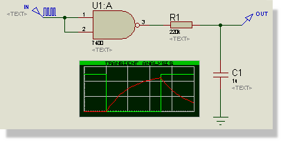
A 7400 with no explicit power supply connections
All these problems are solved by the introduction of the ITFMOD component property. This is very similar to the MODEL property in that it provides a reference to a set of property values but it also activates a special mechanism within the netlist compiler. Essentially this works as follows:
- For any device that has an ITFMOD property an additional model definition is called up during netlisting that will specify control parameters for ADC and DAC objects, and also the pin names of the positive and negative power supplies. In the above circuit, U1:A will have ITFMOD=TTL.
- Having obtained the names of the power supply pins (VCC, GND in this case), the netlist compiler creates a special primitive and connects it across the power supply pins. It names this object similarly to an object on the child sheet or model, so that in the above circuit, the power supply object will be called U1:A_#P.
- When PROSPICE
simulates a mixed mode circuit, it creates ADC
and DAC
objects and considers them to belong to the objects to which they
connect. In the case of the circuit above, a DAC
object will be created with the name U1:A_DAC#0000 because
it forms the interface from U1:A's output.
The clever part is that on doing this, it also looks for a power supply interface object with the same name stem, that is U1:A, and finds U1:A_#P. It then instructs U1:A_DAC#0000 to take its properties from U1:A_#P which in turn has inherited its properties from the model specified in the original ITFMOD assignment. Thus the DAC object operates with parameters defined for the TTL logic family. - The power supply interface object also connects to the same voltage rails as its parent part and the digital device totem pole outputs can thus be modelled much as in real life, sinking or sourcing current from the device power supply rails.
Where an interface object has no power supply object of its own to inherit from, its V+ and V- pins are connected to the design's VCC and GND nets instead. That fallback works for the great majority of designs but breaks down where several different supply voltages are in use, so a part that matters should carry its own interface model.
It is also possible to give the design as a whole an interface model, by defining one under the bare name #P rather than a per-part <part>_#P. Every interface object that has no closer match then inherits from it.
If an interface model names power supply pins that the part does not have, the power interface cannot be connected and the simulation log carries:
V+/V- pins not specified for power interface - check ITFMOD properties.
Using ITFMOD Properties
The following interface models are defined for the standard logic families:
| Family | Description |
TTL |
Standard TTL (74 series) |
TTLLS |
Low Power Schottky TTL (74LS series) |
TTLS |
Standard Schottky |
TTLHC |
High Speed CMOS TTL (74HC series) |
TTLHCT |
High Speed CMOS TTL with TTL outputs (74HCT series) |
CMOS |
4000 series CMOS |
NMOS |
Microprocessor type MOS circuits with TTL logic levels |
PLD |
PLD type MOS circuits |
RS232 |
RS232 line levels, with outputs at -8.5V and +8.5V and correspondingly lowered input thresholds |
A second group of definitions supplies the characteristics of the processor families. These are the models the VSM microcontrollers use, and they are the ones to copy from if you are writing a model of your own for a device in one of these families. The supply pin names differ between them, which is the usual reason for choosing one rather than another.
| Family | Supply pins | Description |
PIC |
VDD, VSS |
PIC microcontrollers at 5V logic thresholds |
PIC3V3 |
VDD, VSS |
PIC microcontrollers at 3.3V logic thresholds |
8051 |
VCC, GND |
8051 family devices |
AT89 |
VCC, GND |
AT89 series 8051 derivatives |
STC15 |
VCC, GND |
STC15 series 8051 derivatives |
AVR |
VCC, GND |
AVR microcontrollers |
MSP430 |
VCC, GND |
MSP430 microcontrollers |
PICCOLO |
VCC, GND |
Piccolo digital signal controllers |
CM0 |
VCC, GND |
Cortex-M0 devices |
CM3 |
VDD, GND |
Cortex-M3 devices |
CM3NXP |
VDD, VSS |
Cortex-M3 devices which name their supply pins VDD and VSS |
CM3STM |
VDD, VSS |
Cortex-M3 devices from STMicroelectronics |
CM4 |
VDD, VSS |
Cortex-M4 devices |
LPC2100 |
V3, VSS |
LPC2100 series ARM7 devices, whose logic supply pin is named V3 |
BSTAMP |
VDD, VSS |
BASIC Stamp modules |
It follows that any new digital model can be assigned a device family by adding a property such as
ITFMOD=TTL
The family definitions are held in the file ITFMOD.MDF which is kept in the models directory. It is a plain text file and is the authority for what each family does, so if you need the exact rise time or threshold voltage a family specifies, read it there.
Each definition can contain any or all of the properties defined for the ADC and DAC interface primitives. In addition, the following may be given:
| Property | Default | Description |
V+ |
none |
Name of the positive power supply pin. |
V- |
none |
Name of the negative power supply pin. |
VOLTAGE |
5 |
The operating voltage of the internal battery, in Volts. |
RINT |
1m |
The impedance of the internal battery, in Ohms. The default is 1m where VOLTAGE is non-zero and 1k where it is zero. A value of zero disables the battery altogether. |
FLOAT |
none |
Specifies HIGH or LOW as the state taken by floating inputs. Where it is not given, floating inputs are Undefined. |
Finally, it is worth pointing out that any specific property, TRISE for example, can be overridden on the parent device, so if you want to simulate a 4000 series IC with a slow rise time, you could add TRISE=10u directly to its property list. FLOAT is the one worth stating explicitly: a FLOAT property on the part is resolved first and takes precedence over the value the interface model supplies.
See Also: