Pads & Padstacks
Overview
Proteus PCB Layout features a sophisticated and flexible system for defining shapes and sizes for pads.
Each pad is given a unique style name, and this name is then used to refer to the style whenever it is used. The dimensions and other characteristics for each style are held in layout-global table, and this makes it possible to change the dimensions of all the pads or tracks in a particular style extremely easily. At the same time, the use of names means that there is no serious limit on the number of pad types that you can have per layout.
Pad Styles
Proteus supports 7 types of pad, namely:
- Circular PTH
- Square PTH
- DIL PTH
- Circular SMT
- Rectangular SMT
- Polygonal SMT
- Edge Connector
and the list of styles defined for each tyreope displays in the Object Selector whenever the appropriate pad icon is highlighted.
When one of these lists is displayed, you can edit an existing pad style by highlighting it in the selector and then clicking the Edit button. All fields on the resulting dialogue form have context sensitive help associated with them.
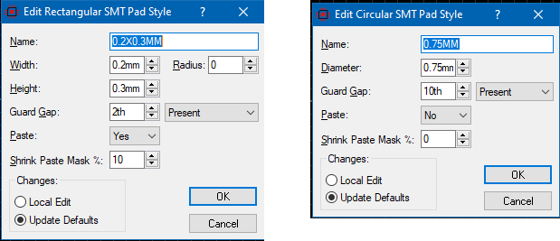
Editing a SMT pad style and Editing a Circular PTH pad style
The Edit Pad Style dialogue is the place to set control of paste mask and solder mask opening (guard gap) for your pads. These pad styles can then be saved into the global style library and will apply to future projects.
Plated or Unplated Status
Through hole pads are all plated by default. You can mark a loose pad as unplated by:
- Place the loose pad onto the layout.
- Right Click > Edit Properties.
- Switch to unplated in the resulting dialogue form.
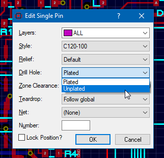
Specifying a particular pad on the layout as unplated.
Slots
Proteus supports slots as both part of a pad and as a user drawn cutout on the board.
Slotted Pads
Slotted pads are created as a type of padstack with the definition of a slot width, height and slot tool.
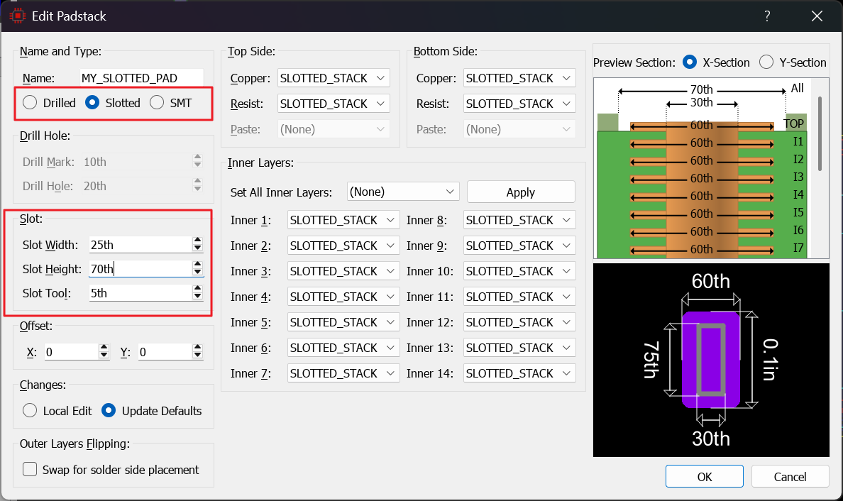
Defining a Slotted Padstack
Slots are rendered in gerber by 4 strokes (DRAW) of the tool. A thin tool option is generally better as it will leave less rounded corners. Regardless, your choice of slot tool is important, so use the preview on the right hand side for a guide.
When choosing slot dimensions, keep in mind that most board houses specify a minimum tool diameter for milling slots, typically around 0.8 mm (32 thou). Narrower slots may not be manufacturable or may attract extra charges. It is good practice to confirm tool limits with your chosen manufacturer before finalising padstack slot sizes.
Plated or unplated
By default, slotted padstack holes are plated. You can edit them and make them unplated after placement from the right click context menu.
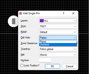
Defining a slot to be unplated.
Output
For Gerber X2 output, slotted padstacks will be output in the appropriate plated or unplated drill file, carrying a ComponentDrill or MechanicalDrill aperture function according to their plating.
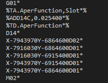
Example Slot output
As mentioned above this slot is created by four DRAW operations (D01), with the initial operation being a move to (D02).
Perhaps surprisingly, in Gerber X2 mode padstack slots do not output in the profile file, which is reserved for board cutout slots. Holes in the board itself, including the board edge, are defined in the Profile layer whereas holes in pads, of any type, are in the appropriate drill file. In RS274X mode the slot is also drawn on the slot layer, so it does appear in the profile output there.
Board Cutout Slots
These consist of graphics objects (normally lines or rectangles) drawn on the slot layer. Think of three lines around a temperature sensor acting as thermal cutoff or an actual square cutout in the board. To place, simply select the appropriate 2D graphic tool, change the layer to slot and draw as needed.
Clearances from these objects to other copper features is defined in design rule manager under Edge/Slot Clearance. Output of board cutout slots takes place in the profile file, includes the board edge itself and is deemed unplated.
Polygonal Pads
Proteus supports a user defined, polygonal pad style in order to cater for parts requiring unusual pad shapes.
To define a new polygonal pad style
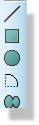
- Using the 2D graphics Line, Arc or Path icons, draw a closed path to define the shape of the new pad style. It does not matter which layer you draw on for this purpose.
- Place an Origin marker within the closed path to specify the origin of the pad style. The origin is used as the connection point for tracking, and also serves as the point of alignment if the pad style is used within a pad stack.
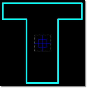
Note that the origin must lie within the closed boundary i.e. within the copper area of the pad. - Tag the 2D graphics and origin marker by drawing a tag-box with the right mouse button.
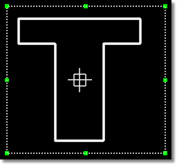
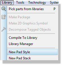
- Invoke the New Pad Style command from the Library menu.
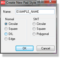
- Enter a name for the new pad style.
- Set the Polygonal pad style type under SMT.
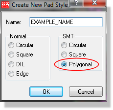
- Click OK.
- Configure the paste mask and guard gap (solder mask opening) as required.
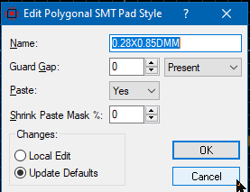
- If you wish to create the style only in the current layout, and not in DEFAULT.STY, then select Local Edit instead of Update Defaults.
- Click OK to create the new pad style.
It is worth noting that zones will connect thermally to the origin of the pad and not the centre of the pad.
Pad Stacks
The ordinary through hole pad styles can be placed on a single layer or on all the copper layers, but this does not provide a very convenient or satisfactory method for defining component pins which have different pad shapes on different layers. In particular, the connectivity system does not recognise connectivity between single layer pads on different layers.
Instead, Proteus provides the facility to define Pad-Stacks. There are several points about a pad stack:
- A pad stack can have a circular hole, a rectangular slot or be surface only. The latter type of pad stack is used where you wish to defined explicit styles for the solder resist and/or paste mask apertures.
- For each layer, you can assign a different pad style, or no pad. If you choose a pad style then the value for the layer chosen will be taken from that pad style. For example, choosing a C50-30 on top resist will take the resist setting from the C50-30 style (5 thou) and apply it to top resist in the pad stack.
- For obvious reasons the hole or slot diameter of a pad stack is the same for all layers. This is specified at the left hand side of the dialogue form.
- You must use a pad stack to create a pad shape with a slotted hole. You cannot specify a slotted hole in an ordinary pad style.
- The Swap for solder side placement checkbox, in the Outer Layers Flipping group at the bottom of the form, enables the top and bottom layers, along with their solder and paste, to be flipped when the component is placed solder side. It is off by default, so a padstack is not flipped unless you ask for it. Under no circumstances are inner layers flipped.
- For drilled or slotted padstacks, the hole or slot can be offset from the pad origin. This is needed for components such as USB connectors where the mounting pin hole is not centred within the copper pad.
To define a new pad stack
- Select the New Pad Stack command from the Library menu.
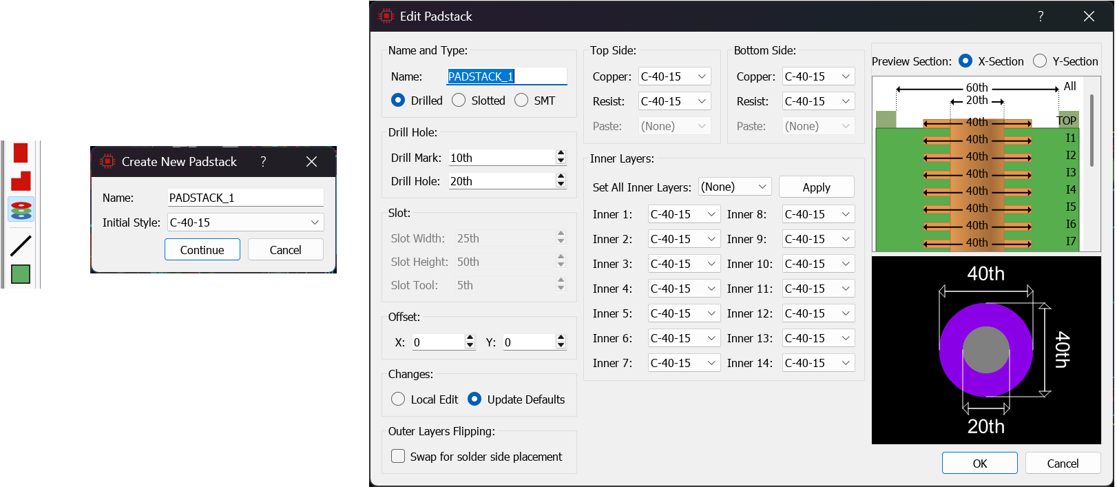
- Enter a name for the pad stack, and a default pad style. All layers will start out with this style of pad.
- Click Continue to proceed to the Edit Pad Stack dialogue.
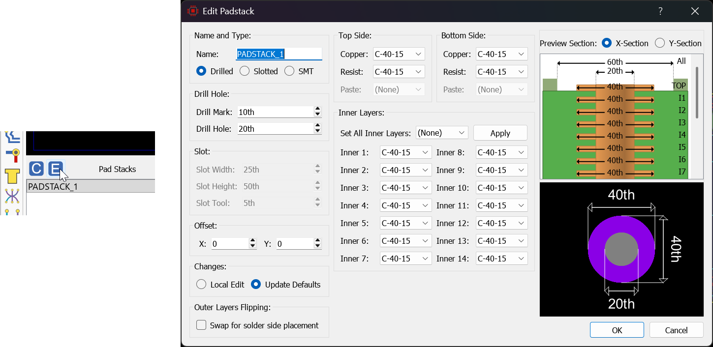
- On this form, you can adjust the pad-layer assignments, and also assign the layer-global drill mark and drill hole/slot size.
The live preview to the right allows you to see either an X or a Y cross section of the resulting padstack. Clicking on a layer in the top graphic will render the pad shape on that layer in the bottom graphic. Turning layers off with the Edit Layer Colours/Visibility command on the View menu (Ctrl+L) will remove them from the graphics in the padstack dialogue form.
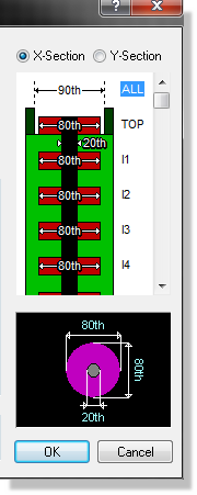
The padstack cross-section preview, showing the pad shape on the selected layer.
To edit an existing pad stack
- Select the Pad Stack icon.
- Select the pad stack you want to edit from the Object Selector.
- Click the Edit button on the Object Selector to bring up the Edit Pad Stack dialogue form.
Off-Centre Holes
In some components the drilled hole or slot is not centred within the copper pad. This is common in connectors such as USB Type-A receptacles and RJ-45 jacks, where shield or mounting pins have a mechanical offset between the hole centre and the surrounding copper annular ring. It also arises in press-fit connectors where the hole is intentionally offset for mechanical alignment purposes.
Proteus supports this by allowing you to specify an X and Y offset for the hole or slot within a padstack. The offset displaces the drill hole (or slot) from the pad origin while leaving the copper annular ring, solder resist opening and paste mask centred on the pad origin.
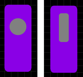
A padstack with an off-centre drill hole, typical of a USB connector shield pin.
Configuring an Off-Centre Hole
Off-centre holes are configured in the Edit Padstack dialogue form. The Offset group provides X and Y fields that specify the displacement of the hole or slot from the pad origin. This group is enabled when the padstack type is set to Drilled or Slotted, and is disabled for SMT padstacks which have no hole.
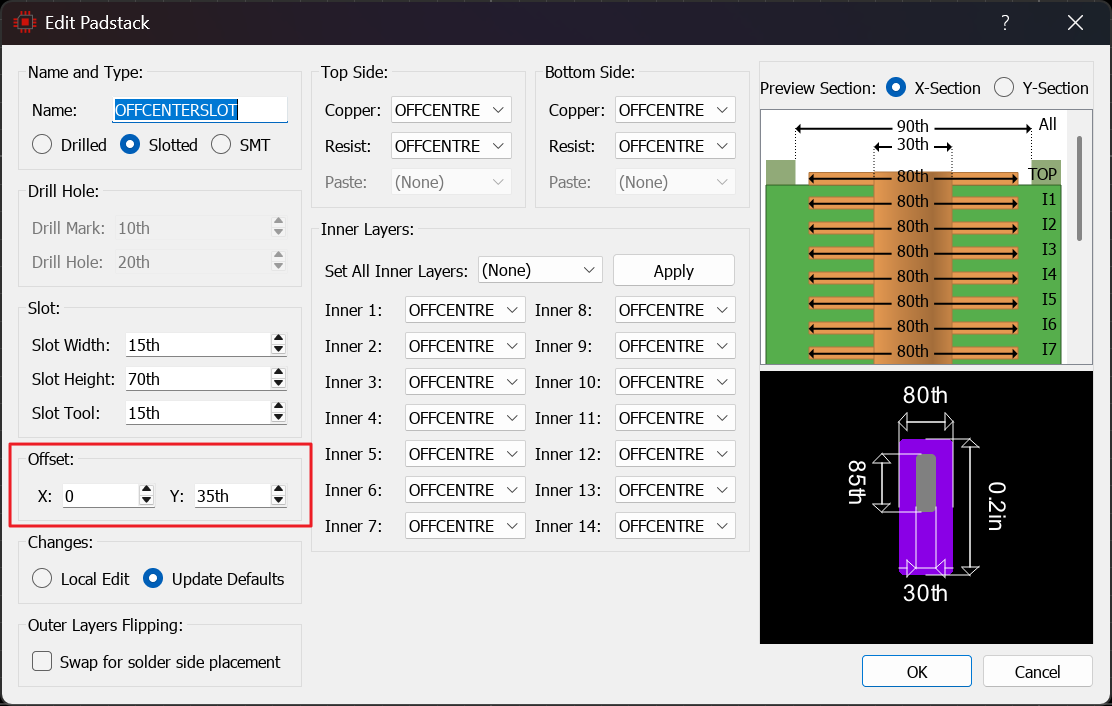
The Edit Padstack dialogue showing the Offset group with X and Y fields.
Enter the desired offset in each axis. Positive X moves the hole to the right and positive Y moves it upwards, relative to the pad origin at zero rotation. When the component is rotated or flipped during placement, the offset rotates and mirrors accordingly.
The cross-section preview on the right of the dialogue form updates in real time as you adjust the offset. Use both the X and Y section views to verify the hole position relative to the copper on each axis.
Design Rule and Zone Behaviour
Design rule checking accounts for the offset position of the hole. Clearance violations are computed from the actual hole location, not from the pad origin. Similarly, zone relief connections and zone clearances are calculated relative to the offset hole centre.
The solder resist opening around the hole also follows the offset. Where a padstack has a guard gap defined on its resist layer, the resist aperture around the hole is generated at the offset position with the appropriate expansion.
Imported Pads
When importing designs from other EDA tools (for example PADS), off-centre slot and hole data is preserved. The importer maps the external offset information to the padstack offset fields so that the imported footprint matches the original design. Imported slotted pads may have zero slot width or height where the slot dimensions match the drill tool diameter exactly.
Only orthogonally-oriented slots can be imported. Where the source design contains a padstack whose slot is rotated to an arbitrary angle, the importer reports that padstacks with rotated slots are not supported and the slot is not brought across. Check any such footprint by hand after import.
Manufacturing Output
Off-centre holes and slots are output correctly in all manufacturing formats. The drill data in both Gerber X2 and RS274X Excellon files reflects the offset position of the hole relative to the component origin. No special configuration is required; the offset is applied automatically during output generation.
See Also:
Gerber Output: Drilling Information Files
Mounting Holes
A mounting hole can be placed as just a loose pad on the PCB. You can then edit the pad and set to drill hole only, thereby removing any annular ring around the hole.
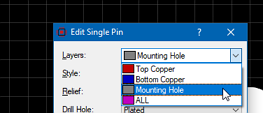
Editing a circular pad and removing the annular ring.
Mounting Holes and Design Rules
When you change the pad to be a mounting hole the design rule that applies becomes Edge/Slot Clearance, since there is no longer any annular ring and so the pad rule does not apply. While unusual you can if needed also set a specific value for zone clearance. If you do this the largest of the following 3 numbers will apply:
- The relevant Edge/Slot Clearance rule.
- Any object clearance specified on the Edit Zone dialogue.
- The value entered in the Zone Clearance field for this particular pad.
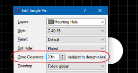
Pad Specific Clearance to a power plane.
Unless exceptions are needed it's best to manage the clearance entirely with design rules. Remember that regional clearances are catered for using design rule rooms.
Pad Styles and the Solder Resist Layer
The solder resist artworks are generated automatically from the pad shapes present on the top and bottom of the board. Each pads' radius is enlarged by the amount specified in the Guard Gap field of its style, as shown below:
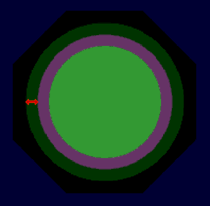
The pad radius enlarged by the Guard Gap to form the solder resist aperture.
Note that in the case of a pad stack, you can define the pad style used for the top and bottom resist layers explicitly, using the selectors in the Edit Pad Stack dialogue form. Note that the guard gap of this style is still applied in determining the final size of the aperture.
You can also specify a pad style which has no solder resist by changing the setting to 'Not Present'. In this case the pad will be covered by the resist coating. If need be, a custom graphic can then be placed on the appropriate resist layer to define the resist escape. This is shown in the movies linked below and covered in more detail in the layout tutorial.
If you are working in hardware accelerated mode (OpenGL or Direct2D) you can turn on live display of the resist mask layer to inspect coverage using the Edit Layer Colours/Visibility command (Ctrl+L). Bear in mind that resist and paste are inverse plots so 'no-coverage' on the layout equates to flood over physically, a 5 thou expansion on the layout equates to a 5 thou gap on the physical board, and so on.
It is important to be consistent with design rules and guard gap (solder mask expansion). Since the Pad-Trace design rule dictates how close a trace can come to the pad and the Guard Gap dictates the solder clearance around a pad, you can end up with slivers of exposed copper if the two settings are inconsistent. In most cases, this will be picked up by the Resist-Trace clearance rule.
See Also:
Layout Tutorial : Hardware Accelerated Display
Creating Advanced Footprints: QFN with Thermal Pad.
Creating Advanced Footprints: Button Pads and Touch Pads
Pad styles can be edited once created by selecting the relevant pad style icon and then the Edit button above the object selector. You can then change the resist for that pad style (guard gap field) and limit the change to the specific layout you are working on by selecting the 'Local Changes' option at the bottom of the dialogue form. This is commonly done when you wish full resist coverage over vias on the layout.
Pad Styles and the Paste Mask
The paste mask artworks are also generated automatically from the SMT pads present on the board. By default, the paste mask aperture is exactly the same as that used for the pad itself although you can specify a shrink percentage in the edit pad style dialogue form if you want it to be smaller. Once again, in the case of pad stacks, different pad styles may be specified explicitly for this purpose.
You can specify a pad style which has no paste mask via the pad style dialogue form. This is useful when creating button pads or touch pads, for example.
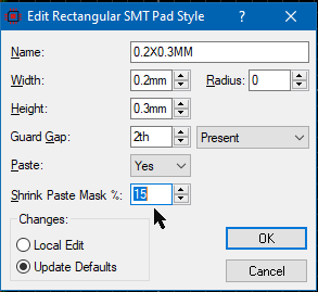
Turning the paste mask off for a pad style in the edit pad style dialogue.
Summary:
- Default for SMT pad styles is paste mask same size as pad.
- You can make it uniformly smaller via the edit pad style dialogue.
- You can turn it off completely via the edit pad style dialogue. This allows you to create custom paste definition with solid 2D graphics blocks (e.g. stippled paste mask on a large QFN centre pad).
The movie links below will help you when you really have no choice but to create your own footprints. We'd advise however that you try the integrated web search first as it may save you a great deal of time.
Creating Advanced Footprints: QFN with Thermal Pad (Stippled Paste Mask).
Creating Advanced Footprints: Button Pads and Touch Pads
If you are working in hardware accelerated mode (OpenGL or Direct2D) you can turn on live display of the paste mask layers to inspect coverage using the Edit Layer Colours/Visibility command (Ctrl+L).
Fiducials
Fiducials are represented in Proteus as pad styles with the name prefix FIDUCIAL. You can have multiple fiducial styles for global and local fiducials (e.g. FIDUCIAL_GLOBAL, FIDUCIAL_LOCAL) or just different styles for different diameter fiducials (e.g. FIDUCIAL20, FIDUCIAL30, etc.).
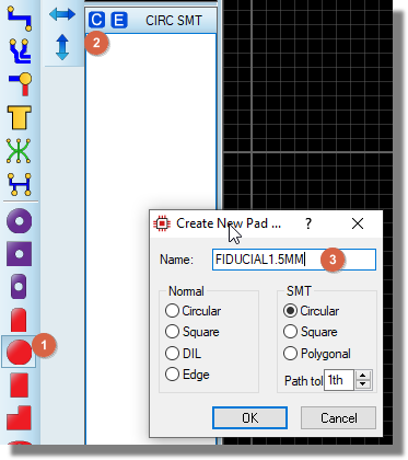
Creating a fiducial pad style using the FIDUCIAL name prefix.
The important points about creating these styles and using them are that a fiducial style is given a 1 mm solder mask guard gap by default, rather than the 5 thou that other pad styles get, and that the output systems can identify the pads as fiducials. You are free to change the guard gap in the pad style afterwards. Gerber X2 for example is capable of tagging fiducial pads as fiducials, fiducials are excluded from the paste mask, and the Proteus manufacturing report can output the co-ordinate positions of all fiducials which can be helpful for insertion machines.
See Also:
Manufacturing Report : Fiducials.
Pads, Power Plane Clearances and Relief Styles
Regardless of the pad style, you can configure both clearance from zones or relief type/style to the zone.
Clearance from a Pad to a Power Plane
There are several contributing factors:
- The zone dialogue contains fields for relief and clearance. These are defaults for all pads encompassed by the zone.
- The Design Rule Manager allows you to set design rules for a net with respect other nets. If such a rule exists for a net with a clearance higher than that in the zone then this value will be applied to all pads on the zone which are connected to the net.
- For a loose pad (e.g. Mounting hole) you can edit the pad and specify a specific minimum zone clearance.
The rule is that the largest value is applied for any pad.
Relief Styles from a Pad to a Power Plane
As with clearance the Edit Power Plane dialogue contains a relief field which allows you to specify the type of connection to make for pads on the same net as the Power plane. This will be the default, although you can right click on any pad and select the Edit Pin dialogue to change the behaviour for a particular pad (E.g. Thermal '+' to Thermal 'x').
See Also:
Example: Specifying the Default Clearance for the Power Plane
Example: Setting the Minimum Clearance for a Pad
Example: Changing the Topology of Relief Stems on a Pad
Example: Specifying the Thickness of Thermal Relief used in Power Plane Connections
Style Management
When you start a new layout, an initial set of styles appears and these come from a system file called DEFAULT.STY which is kept in the "Library" directory of your Proteus installation. This file contains a selection of common pad styles that we feel you may find useful.
When you create or edit pad style you will see that the dialogue form contains a Changes groupbox. If you select Local Edit then only the copy of the style maintained within the layout will be modified. If you select Update Defaults then DEFAULT.STY will also be updated.
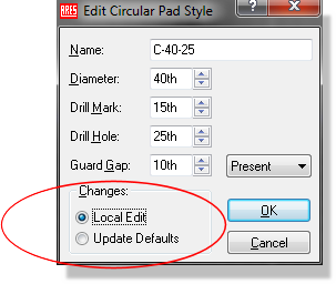
The Changes group box, offering Local Edit or Update Defaults.
Package library parts contain their own copies of styles used by their pads. When the package is brought into a layout for the first time, the style definitions will be taken from the library part if they do not already exist within the layout.
Default Styles Editor
You may find that over a long period of usage, pad, via and trace styles get made that are no longer needed. You can end up with quite a long list in the object selector for a new project, where perhaps half of the pad styles will never be needed again. You can delete pad, via and trace styles from the DEFAULT.STY file with the Edit default styles command on the Library menu:
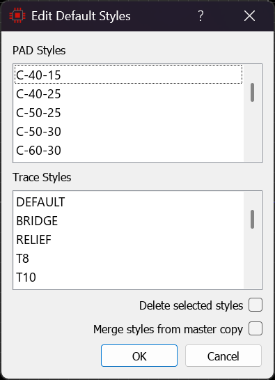
The Default Styles Editor, listing the styles held in DEFAULT.STY.
Delete selected styles
Select a pad style, or several styles, then tick Delete selected styles and click OK.
The styles will be deleted permanently.
Merge styles from master copy
This will load the default styles that are shipped with the software.
The Default Styles Editor works on DEFAULT.STY, which governs what appears in future layouts. To prune the style list of the layout you are working on, use the Delete button above the object selector instead: it removes the highlighted pad, via or trace style provided it is not in use anywhere on the board. See Selector Buttons.