VIA EXAMPLES
Introduction
The examples below cover a range of common via tasks in Proteus, from basic placement during routing through to micro-via usage on HDI boards. For general information on via styles, via filling and non-functional pads, see the main Vias topic.
Pre-Requisites
It is assumed in all of the following examples that you have the following in place:
- Layer stackup, so that the software knows how many copper layers exist and what drill spans are available. Without this, the smart via algorithm cannot select the correct drill range for a via.
- Layer pairs, which determine which layer you transition to when you place a via during routing. They should be set up on the Technology menu before you begin.
- Net class configuration, since the via style used during routing comes from the net class assigned to the net being routed. Setting up net classes in the Design Rule Manager ensures that each net uses the correct via dimensions automatically.
Example: Placing a Via when Routing
The most common way to place a via is during route placement, when you need to transition from one copper layer to another.
- Select Trace Mode.
- Left click on the starting pad and begin routing.
- Double click the left mouse button to place a via and continue routing on the paired layer.
- Route to the destination pad and left click to complete the connection.
Key Points
- The via style comes from the net class of the net being routed.
- The drill span is selected automatically by the smart via algorithm, which finds the shortest compatible span between the source and destination layers.
- The destination layer is determined by the layer pair configuration for the current layer.
- Both the via style and drill span are defaults, so you can edit the via afterwards to change either.
Example: Controlling the Exit Layer when Routing
When routing on a multilayer board you may need precise control over which layer a via transitions to, rather than accepting the default layer pair.
- Select Trace Mode and begin routing from the starting pad.
- Use PGUP and PGDN to cycle through the valid layer destinations for the current position. The layer selector follows, showing the layer the route will continue on.
- With the layer you want selected, press SPACE to place a via and continue routing on that layer.
- Route to the destination and complete the connection.
Key Points
- Cycling the layer with PGUP and PGDN overrides the default layer pair for this via only; it does not change the layer pair configuration.
- The destinations offered are limited to the layers reachable by the drill spans defined in the layer stackup.
- With smart vias enabled you choose the layer and Proteus chooses the span: the best drill span for the transition is selected automatically at the end of the route.
- This technique is essential for BGA escape routing where different signals need to exit on different layers.
See Also:
Manual Routing Example: Routing Across Multiple Layers
Example: Changing a Via Style after Routing
The via style and drill span assigned during routing are defaults. You can change them on any placed via using the Edit Via dialogue.
- Right click on the placed via.
- Select Edit Via from the context menu.
- Change the via style, drill range, or other properties as required.
- Click OK to apply the changes.
Key Points
- You can change any via to any compatible style after placement, since the style chosen during routing is a default rather than an enforced constraint.
- If you change a via to a micro-via style, the drill span must be a lasered (micro-via) span defined in the layer stackup, and vice versa.
- The filled checkbox is automatically set and locked for micro-via styles. For through-hole vias, you can set or clear the filled status from this dialogue.
Example: Altering a Via Style and Applying to Placed Vias
If you need to change the dimensions of an existing via style and apply the change across the board, the Via Inspector provides the tools for bulk editing.
- Open the Via Inspector from the Tools menu (or from Via mode).
- The table shows all via styles in use on the board, grouped by style name. Click on the style you want to modify to select all vias of that style.
- Edit the via style itself by highlighting it in the object selector in Via mode and clicking the Edit button. Changes to the style definition apply to all vias using that style.
Key Points
- The Via Inspector groups vias by style name and drill range, making it easy to see how many vias of each type exist on the board.
- If you edit a via style, for example changing the hole size from 0.3 mm to 0.4 mm, the style name will no longer reflect the dimensions. It is good practice to rename the style to match, or create a new style with the desired dimensions and use the Via Inspector to reassign vias to it.
- The Via Inspector also provides bulk operations for NCVF, Via-in-Pad and NFP removal.
See Also:
Example: Using Micro-Vias
Micro-vias are laser-drilled vias used on HDI boards, typically to escape from fine-pitch BGAs through the outer buildup layer. Because micro-via styles are not available in the net class dialogue, placement during routing is controlled exclusively through DRC Rooms. This example walks through the full setup.
Setup
- Configure the layer stackup as a 1+n+1 HDI board using the Layer Stackup dialogue on the Technology menu. Ensure that a lasered (micro-via) drill span is defined between the outer copper and first inner copper on each side.
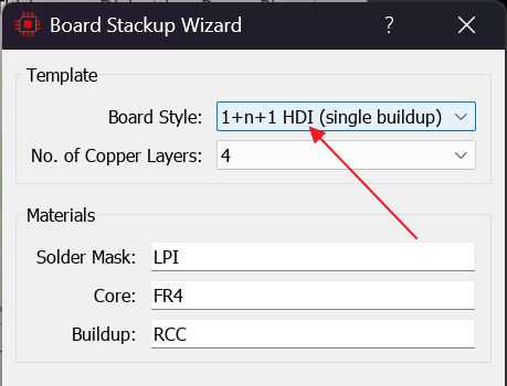
A 1+n+1 HDI layer stackup with a lasered drill span between the outer and first inner copper layers.
- Create a micro-via pad style (for example a 0.1 mm hole with a 0.25 mm pad) using the New Via Style command on the Library menu. Set the Laser Drilled (HDI) option in the style properties.
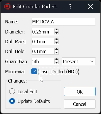
Creating a micro-via style with the Laser Drilled (HDI) option set.
- Place a DRC Room around the BGA footprint area. In the room properties, set the via style override to the micro-via style you created.
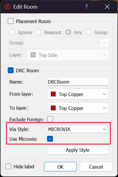
A DRC room with its via style override set to the micro-via style.
Routing
- Select Trace Mode and begin routing from a BGA pad.
- Double click to place a via. Because you are inside the DRC Room, the software overrides the net class via style with the micro-via style and selects the lasered drill span automatically.
- Route on the inner layer to escape the BGA area. When you exit the DRC Room and place further vias, they revert to the standard mechanical via style from the net class.
Key Points
- Micro-via styles cannot be selected in the net class dialogue. The DRC Room is the exclusive mechanism for placing micro-vias during routing.
- The smart via algorithm automatically selects the lasered drill span when the active via style is a micro-via, and excludes lasered spans when it is a standard mechanical style.
- Micro-vias are always filled and capped (IPC-4761 Type VII) as part of the HDI fabrication process. This is set automatically by Proteus and cannot be changed.
- If you need micro-vias along an entire net but cannot specify them in the net class, route the net with standard vias and then edit the vias afterwards to change them to micro-via styles.
See Also:
Example: Auditing Micro-Vias before Output
On HDI boards, it is good practice to verify micro-via compliance before generating CADCAM output. This example shows how to use the drill table and Microvia Compliance report together.
- Open Project Notes and select the manufacturing report (or create one from the PCB Manufacturing Report template).
- Ensure the report contains a Drill Table data object. This provides a summary of all hole sizes, types and layer spans on the board including micro-vias.
- Insert a Microvia Compliance data object from Insert > Project Data. This audits every micro-via against three criteria: drill span validity, filled status and aspect ratio. The aspect ratio warns above 0.75:1 and fails above 2:1.
- Review the compliance report. Any micro-via that fails a criterion is listed with the reason. Fix issues in the layout, for example using the Via Inspector or Apply Style, and regenerate the report until it passes.
- Run the Pre-Production Checklist for a final pass/fail summary including all micro-via checks.
Key Points
- The drill table documents what will be fabricated; the compliance report verifies that the micro-via configuration is correct. Both should be included in the manufacturing pack for HDI boards.
- The Pre-Production Checklist runs the compliance report's three checks and more besides, among them a check that each micro-via's style is consistent with the DRC room it sits in. Use the data object for per-via detail in the manufacturing pack and the checklist for the broader pass/fail summary.
- The compliance report can be regenerated at any time from the right click context menu to reflect the current board state.
Example: Via-in-Pad
Via-in-pad is a technique where a via is placed directly in a component pad, most commonly under BGAs. This maximises breakout density but usually requires the via to be filled to prevent solder wicking down the hole during reflow.
- Select Trace Mode and begin routing from the component pad.
- Double click directly on the pad to drop a via in the pad location.
- The via is placed coincident with the pad centre, forming a via-in-pad.
- Apply the filling. A through-hole via is placed unfilled, so the fill has to be set deliberately. You can do it from the right click context menu on the via, from the Via Inspector's Via-in-Pad button for a group of vias, or from the Filled checkbox in the Edit Via dialogue for a single via.
Placing a via in a pad does not fill it. Unless you set the fill yourself, the board will go to fabrication as an unfilled via-in-pad design and solder will wick down the holes during reflow. Micro-vias are the exception: they are always filled.
The filling options described here apply to CNC drilled through-hole vias. Micro-vias are always marked as filled to the IPC-4761 Type VII standard as part of the HDI fabrication process and this cannot be changed.
Key Points
- Through-hole vias are placed unfilled, whether or not they land in a pad. Set the filled status in bulk using the Via Inspector's Via-in-Pad button, by area from the selection context menu, or individually through Edit Via. The Via-in-Pad button checks that each via geometrically intersects a component pad before changing it, so vias that are not in pads are left unchanged.
- Micro-vias placed in pads (common for BGA escape on HDI boards) are always filled and capped by copper electroplating. This is set automatically by Proteus and cannot be changed.
- There are legitimate engineering reasons not to fill a through-hole via-in-pad, for example during prototyping, on lower density boards, or where the pad is large relative to the hole. See Via Tenting and Filling for more detail.
- Filled via-in-pad vias are output as IPC-4761 Type VII in Gerber X2.
Example: Setting Via Filling (NCVF) by Area
Non-conductive via filling (NCVF) is a resin filling process for CNC drilled through-hole vias. It can be applied to vias in a specific area of the board, for example all the vias under a BGA footprint.
- Enter selection mode and drag a box around the area concerned, for example the BGA with vias in pad.
- Right click inside the selection box and choose Via Filling from the context menu.
- Set the vias to be resin filled.
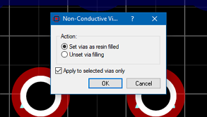
Setting the vias inside a selection box to be resin filled.
Key Points
- NCVF applies to CNC drilled through-hole vias only. The resin fill process (fill, cure, planarise, re-plate) adds cost and lead time to fabrication.
- Micro-vias use a different process (copper electroplating) and are always filled as part of HDI fabrication. Their filling cannot be changed.
- Filled vias are output as IPC-4761 Type VII in Gerber X2. See Output Systems for details.
Example: Setting Via Filling (NCVF) using Via Inspector
The Via Inspector provides a bulk method for setting or unsetting resin filling (NCVF) on CNC drilled through-hole vias, grouped by via style.
- Launch the Via Inspector from the Tools menu or from Via mode.
- Click on the table to select through-hole vias of the style or styles you want to fill.
- Click on the NCVF button underneath the table. A dialogue offers to set or unset filling for the selected vias.
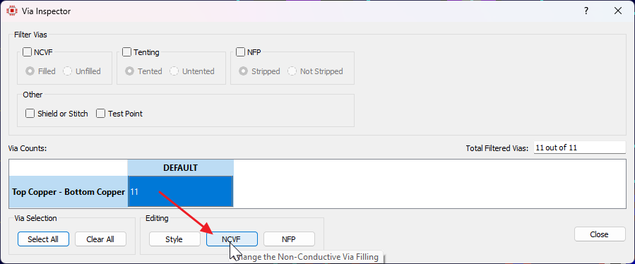
Setting resin filling on the selected through-hole vias with the NCVF button.
Key Points
- The NCVF button is only enabled when CNC drilled through-hole vias are selected. It is disabled for micro-vias (which are always filled by copper electroplating) and for blind and buried vias.
- You can also set or unset the filled status of a single via by right clicking on it, selecting Edit Via, and toggling the filled checkbox.
Example: Setting Via Filling on a Single Via
To change the resin filling status of an individual CNC drilled through-hole via:
- Right click on the via and select Edit Via from the context menu.
- Select or de-select the Filled checkbox.
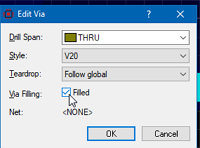
The Filled checkbox in the Edit Via dialogue.
Key Points
- The filled checkbox is available for CNC drilled through-hole vias only. For micro-vias, it is checked and locked (micro-vias are always filled by copper electroplating as part of HDI fabrication).
- For blind and buried vias, via filling is not available.
Example: Viewing Filled Vias on the Board
To see which vias on the board are marked as filled:
- Launch the Via Inspector from the Tools menu or from Via mode.
- Click on the NCVF filter at the top of the dialogue to restrict the results to filled vias only.
- Click on a style in the table to highlight those vias on the layout.
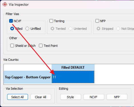
The NCVF filter restricting the data table to filled vias.
The NCVF filter shows all vias that have the filled flag set. This includes both resin filled through-hole vias and micro-vias (which are always filled as part of HDI fabrication). In the data table, filled vias of either type appear in a separate column prefixed with "Filled".
Example: Removing Non-Functional Pads
Non-functional pads (NFPs) are annular rings on layers where a via has no electrical connection. Removing them can free up routing space and reduce parasitic capacitance.
- From the Edit menu, select Remove/Restore Non-Functional Pads.
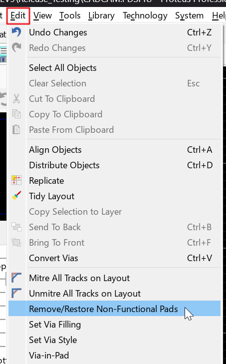
Remove / Restore NFP.
- By default the command applies to the entire board. To limit the scope, first select an area, for example around a BGA, and then run the command: it will apply only to vias within the selection.
Key Points
- The two extremities of the via always keep their annular rings. A through-hole via will always have rings on top copper and bottom copper; a blind or buried via will have rings on the extremities of its drill range.
- Depleted vias are automatically restored on the relevant layer if you route to them manually.
- The autorouter will not connect to a depleted via on a layer with no annular ring.
- A non-functional pad remains a pad for the purposes of design rules. Where only the drill hole remains, the hole edge is the measurement point for clearance rules.
Example: Bulk NFP Removal using Via Inspector
The Via Inspector allows you to remove or restore non-functional pads across the board, grouped by via style.
- Launch the Via Inspector from the Tools menu or from Via mode.
- Click on the style or styles in the table to select vias.
- Click on the NFP button at the bottom and choose to remove or restore unused pads.
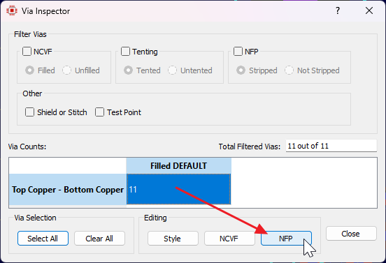
Removing or restoring non-functional pads in bulk with the NFP button.
Example: Viewing Depleted Vias
Depleted vias (vias with non-functional pads removed) are shown with a sliver ring on layers where the annular ring has been removed. This makes them visible when routing with restricted layer visibility.
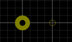
Viewing Inner1 only. The depleted via on the right shows a sliver ring to make it visible.
The sliver ring is only visible when all layers on which the via still has an annular ring are turned off. If any layer with a remaining ring is enabled, the via renders normally.
To view all depleted vias on the board:
- Launch the Via Inspector from the Tools menu or from Via mode.
- Click on the NFP filter at the top of the dialogue to restrict the results.
- Click on a style in the table to highlight those vias on the layout.
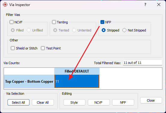
The NFP filter listing the depleted vias on the board.
See Also:
Example: Stitching Two Zones Together
Via stitching ties together copper zones on different layers to maintain a low-impedance reference. This example walks through stitching two power planes.
- Right click on the border of the zone you want to stitch from and select Via Stitch from the context menu.
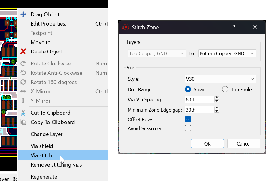
Choosing Via Stitch from the zone border context menu, and the resulting dialogue form.
- If there are multiple planes on different layers, select the destination zone for the stitching. Set the via style and the spacings for the via grid.
- Click OK. It may take up to a minute for the vias to be placed. Vias will appear wherever they fit within the zone boundary.
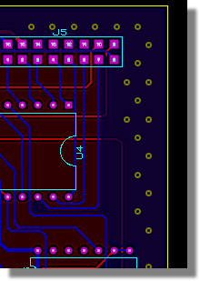
Stitching vias placed across the zone.
Key Points
- Stitching zones should be done towards the end of development because it will render the board almost un-routable.
- Stitching vias are assigned to the zone stated on the left hand side of the dialogue form. To remove them, right click on that same zone and select Remove Stitching Vias.
- If you select the wrong zone for removal, you will see an error in the status bar. Check which zone owns the stitching vias.
- You can also remove groups of stitching vias with a selection box and the selection filter, but be careful not to catch routed vias in the selection.
- Stitching and shielding vias can be reviewed and bulk edited using the Via Inspector, which has a Shield or Stitch filter for the purpose.
See Also:
Stitching & Shielding Zones with Vias
Example: Shielding a Zone with a Via Fence
A via shield or picket fence is a row of vias around the perimeter of a power plane, used to isolate signals or suppress electromagnetic interference.
- Right click on the zone border and select Via Shield from the context menu.
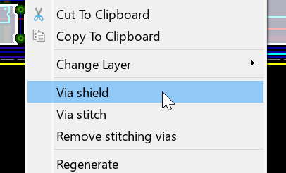
Choosing Via Shield from the zone border context menu.
- Specify the destination zone for the stitch (if more than one is available) and set the spacing requirements for the vias.
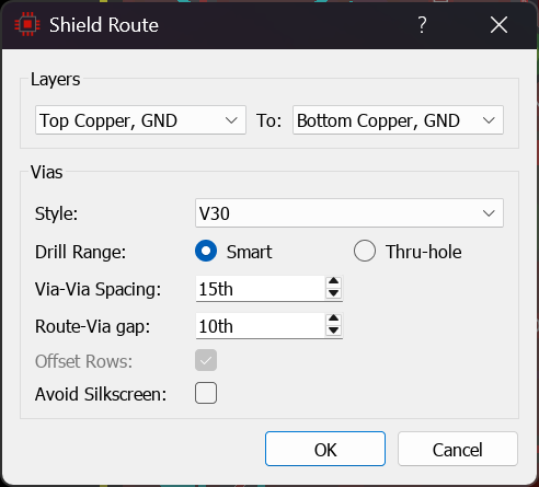
Setting the destination zone and via spacing for the shield.
- Click OK. The shield vias will be placed around the zone perimeter.
Key Points
- A via shield is normally planned early in the design process to ensure there is space around the zone boundary for the fence.
- For shielding fences, a common rule of thumb is via-to-via spacing of no more than a twentieth of a wavelength at the highest frequency of interest, which is approximately 7.5 mm at 1 GHz.
- Only standard mechanical via styles are used for shielding; micro-vias are not available for this purpose.
Example: Shielding Routes with Vias
A via shield can also be placed bracketing one or more routes, forming a coaxial-like guard structure between two power planes.
- Make sure you have power planes in the correct topology on either side of the route for the shielding vias to connect to.
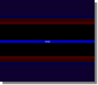
Power planes above and below the route, giving the shielding vias something to connect to.
- Select the route or routes (hold CTRL for multiple selection) and select Via Shield from the context menu. Do not select the zone.
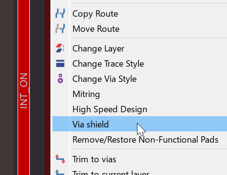
Choosing Via Shield from the route context menu.
- Specify which two zones are being stitched together, the spacing between vias, and the spacing between the vias and the edge of the route.
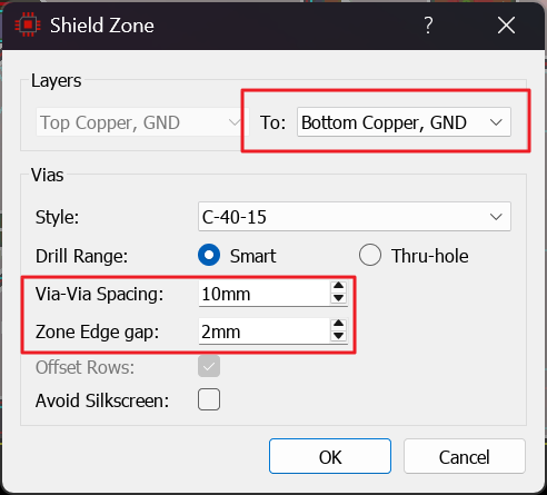
Setting the two zones to be stitched, the via spacing and the via to trace distance.
Key Points
- The via shield takes the edge-to-edge width of all selected routes, expands it by the via-trace distance specified in the dialogue, and places vias between the two specified power planes along the path. If the specified power plane does not exist at this distance from the track ends then nothing will happen.
- You must ensure that power planes exist in the right locations for the shielding vias to connect to.
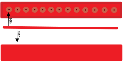
If the via-trace distance places vias where no zone exists, nothing will happen.
See Also: