Design Explorer takes the schematic and displays it in a familiar spreadsheet like editing window. Both a physical view (components) and a connectivity view (nets) are available making it the perfect place for design analysis and block editing operations.
- Spreadsheet like view makes design analysis and property editing easy.
- Cross probe to either schematic or PCB from any design explorer entry.
- Powerful search tools to help filter results and target editing changes.
- Simple interface for creation and management of assembly variants.
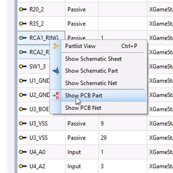
Cross Probing
If you right click on a component in design explorer you can right click on any part and choose to cross-probe to it either on the schematic or on the layout. This will switch tabs to the appropriate module and zoom the view into the component part.
Similarly, if you right click on a pin or a net you can choose to select the net on either the schematic or the layout with the same zoom and highlight result.
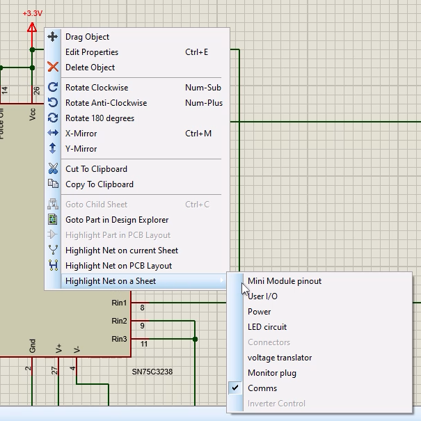
Design Walk
You can select a net from design explorer or by right clicking on a schematic wire. Then the entire design can be walked one sheet at a time with the pgup and pgdown keys with the current net tagged on each sheet.
Alternatively, the context menu will show a list of sheets on which the net is present so can navigate to each relevant sheet manually.
Block Editing
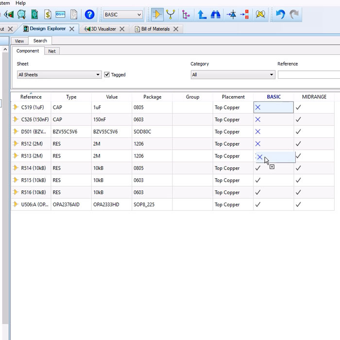
Design Explorer is the perfect place to make bulk edits to the schematic component properties. With a spreadsheet view you can easily see what you are doing and it's both quick and simple to make changes.
Design Explorer also comes with powerful search filter to make it easier to make targeted changes. For example, you might filter the design view down to all 10k resistors before making a bulk packaging change to 0805 footprint
Variant Management
Management of Assembly variants takes place in the main design explorer view. When a new variant is created it becomes a column in the spreadsheet and each component defaults to being fitted. Users can quickly change the fitted status for those parts not in the current variant and can also use the property editing features to swap in alternative, pin compatible parts in the current variant.
 Ask An Expert
Have a Question? Ask one of Labcenters' expert technical team directly.