FLASH memory has become the most popular technology for storing data nowadays, with its low cost and small size. Most microcontrollers use FLASH for their main program memory, external FLASH chips offer an inexpensive way to add additional memory if needed, and the popular SD card also implements FLASH technology; Electronic Engineers are thus bound to work with FLASH memory on a regular basis. FLASH memory has a number of nuances however which are not obvious without prior experience.
FLASH is a non-volatile memory. It is not as fast as RAM, but it remembers its contents when the power goes off. Many embedded projects have a need to save some values to non-volatile memory, such as user settings or log data, and not long ago many microcontrollers included an area of EEPROM memory for this purpose. EEPROM is easy to understand and work with – it contains a certain amount of memory, and each byte can be individually read from and written to (much like RAM, just slower). EEPROM can handle a higher number of erase-write cycles than FLASH, and so was the memory-of-choice for this application. As FLASH technology improved however, and versions with higher erase-write cycle endurance were developed, EEPROM memory disappeared from newer microcontrollers. FLASH memory can also be used for storing settings and logging data, however it has some peculiarities which should be understood when working with it.
Sector Erase
When FLASH memory is erased, all the bits in it are set to 1’s (not 0’s). If you see a lot of 0xFF (hexadecimal for the binary 11111111) when working with FLASH, then that is because the FLASH has been erased. Whilst bits and bytes can be individually flipped from 1’s to 0’s in FLASH, flipping them from 0 to 1 again can only be done in bulk! FLASH memories are organised into sectors (sectors may further be grouped into blocks), with sector size usually being in the order of kilobytes; a sector is the smallest memory area which can be erased at a time. Let’s say you have 100 settings saved to FLASH, and you only want to update setting # 3; in order to do this it is necessary to erase the entire FLASH sector containing setting #3 and then rewrite it – the problem is that this will erase all the other settings as well, so all of them will need to be rewritten too. There are a number of ways to work around this:
- One method is to read all the values back into RAM, erase the sector, and then write them all back again (with the new/updated values). Depending on the size of the settings (or other data, such as log values) and the amount of RAM available, this may not be an option.
- Another method is to copy all of the values to another blank FLASH sector, erase the original sector, and then write the values back to the original sector again (with the new/updated values).
- A similar version of the above method uses two FLASH sectors and 'ping pongs' between them – whenever new values need to be written then they are written to the currently-blank sector, and the old sector is then erased (to be used the next time that it is necessary to write new/updated values).
- When logging data, then a number of FLASH sectors may be used in a circular fashion. New log entries are written into the blank memory after the old entries. As soon as all sectors are full then the oldest one is erased and used to write new data. Some technique needs to be used to remember which sector is the oldest (starting point), such as an incrementing counter written at the start of the sector. This technique can also be used for saving settings, where each version of the settings is logged and then when it comes time to read the current settings values back then it is simply a case of reading the most-recently-logged values; because FLASH erase operations are slow, this technique may be used to speed up operation of the system.
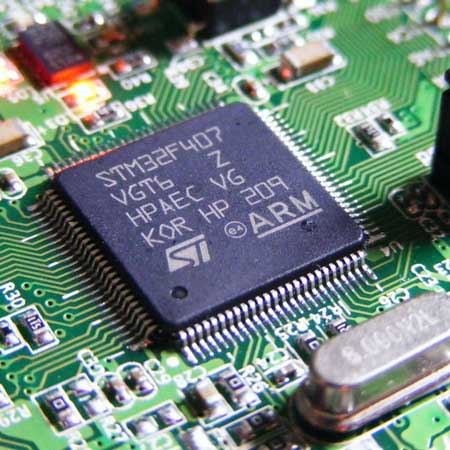
As mentioned above, erasing a FLASH sector is generally a slow operation. Erasing a 128kB sector on an STM32F407 can take between 1 and 4 seconds (depending on supply voltage)! The MCU cannot execute instructions from FLASH whilst an erase is in progress, so this needs to be planned for in the product design, as the product will essentially be unresponsive during that time (there can be alternative options depending on the microcontroller, such as copying program instructions to RAM and executing from there whilst the FLASH erase is in progress – peripherals such as DMA can also continue to operate independently).
Given a good understanding of how FLASH works in general, and knowledge of the parameters of the particular FLASH device being worked with (sector sizes, erase times, etc) from its datasheet, a suitable technique can be implemented to work around the nuances of FLASH and implement the required application.
During a Proteus simulation, it is possible to view the contents of FLASH memory and single-step through operations, which can help to provide insight when developing and debugging projects which work with FLASH memory.
All content Copyright Labcenter Electronics Ltd. 2026. Please acknowledge Labcenter copyright on any translation and provide a link to the source content on www.labcenter.com with any usage.Get our articles in your inbox
Never miss a blog article with our mailchimp emails
Advanced Simulation
Learn more about our built in graphing and advanced simulation features. Harness the mixed-mode simulation engine in Proteus to quickly test your analog or digital circuitry directly on the schematic.
 Ask An Expert
Have a Question? Ask one of Labcenters' expert technical team directly.