Introduction
Charge Pumps are a technique for increasing or inverting a DC Voltage. For example, +5V could be converted to +10V or -5V (or higher / lower values). Compared to boost converters, Charge Pumps require less components and less PCB space, and are cheaper; the limitation of Charge Pumps however is that they are only able to supply relatively small amounts of current.Because of the low-current constraint, Charge Pumps are best suited to applications such as signalling (communications) or driving LCD backlights. A common application, historically, has been the generation of the +3V to +15V and -3V to -15V of RS232 communication transceivers (such as the MAX232).
Theory
The theory of how Charge Pumps work is very simple. One of the first things we learn about electricity is that if we connect batteries in series then their voltages are added.

Another electricity basic is that capacitors are like small batteries.

If we can charge a capacitor with a voltage source and then quickly reposition it in series with the voltage source, then we can double the voltage (in the same way that adding batteries in series adds their voltages). In a circuit, repositioning can be done with switches – either mechanical (physical switches or electromagnetic relays) or solid-state (transistors / diodes).
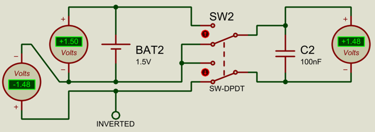
In terms of generating a negative voltage, this is simply a case of repositioning the capacitor so that its positively charged terminal is connected to the negative terminal of the voltage source.

The principle can also be scaled, in that an arbitrary number of capacitors can be charged in parallel at the voltage source and then repositioned in a stack.

Schematic Charge Pump
On the schematic, the above configuration could be done as follows:
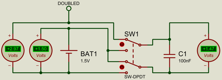 (The screenshot is captured slightly after the moment of switching, at which point the capacitor has already dischared slightly.)
Voltage Inversion would look as follows:
Of course, if there is any load then the capacitor will immediately start discharging, and so it will be necessary to continually switch the capacitor back and forth between the in-parallel and in-series configurations in order to keep recharging it.
To keep the output voltage relatively constant whilst switching, we can add another capacitor at the output.
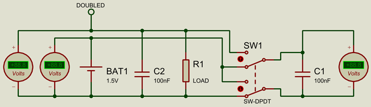
This smooths the output somewhat.
Having someone flip a switch back and forth to run the charge pump is obviously not practical however, and to maintain a relatively-stable-output-voltage with a resonably-sized-capacitor very fast switching is needed; so a fast clock signal to run the switching is required.
Clocked Charge Pumps
In the above circuit, an MC34063 Buck Converter is used to step 25V down to 5V. The switching transistor is integrated inside the controller, and so an external one is not required. The controller monitors the output voltage using the feedback resistors R2/R3, and maintains a constant output voltage at the load.
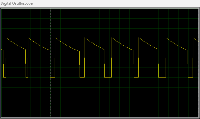
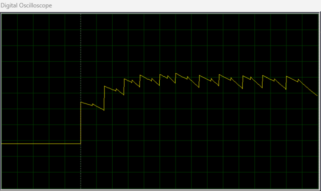
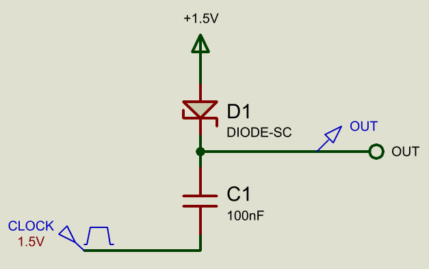
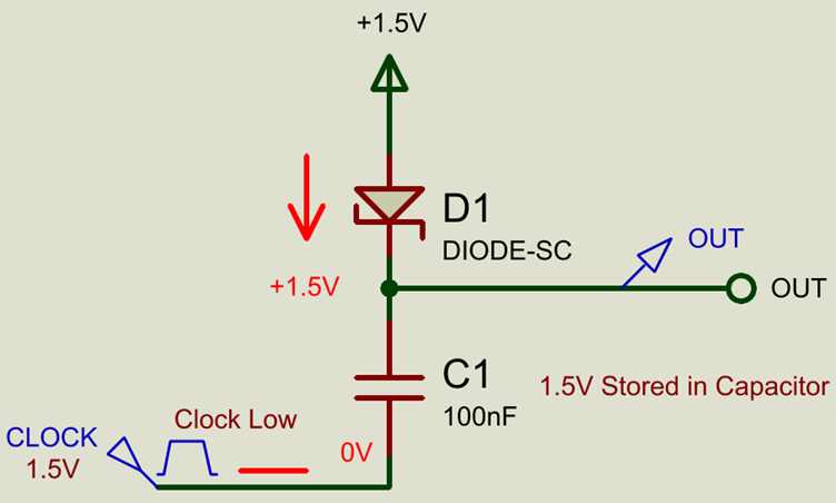
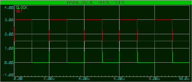
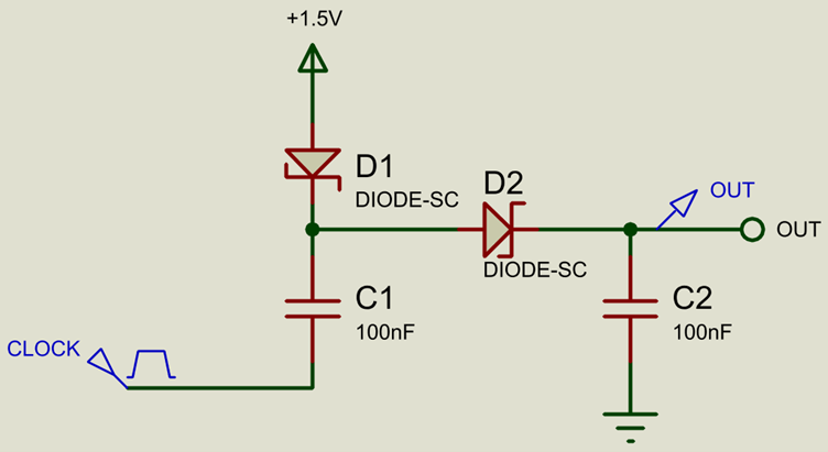
Given a clock signal, we can connect that signal to the negative side of a capacitor and connect the positive side of the capacitor to the positive voltage source through a diode.
When the clock signal is low (0V) then the capacitor will charge through the diode to the positive supply voltage (less the voltage drop over the diode).
When the clock signal is high (supply voltage, +1.5V in this case) then the voltage stored in the charged capacitor will be added on top of the voltage at its negative pin, resulting in a doubled output voltage.
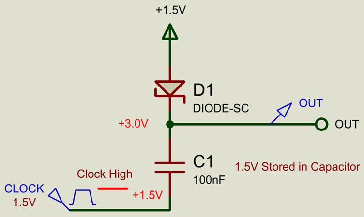 (The diode prevents the capacitor from discharging to the supply voltage.)
The result is that the clock voltage is doubled.
To smooth the output voltage, we can add another capacitor at the output, together with a diode to prevent it from reverse-discharging during the low phase of the clock cycle.
We now have a very smooth output voltage.
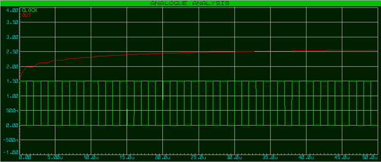
The smoothed output voltage is not quite double the input voltage, due to voltage drops over the diodes (1.5V is very low for a supply voltage and the drop over the diodes is relatively large in proportion – it would be relatively less with a supply voltage of 5V/9V/etc) as well as the non-ideal nature of real-world electronic components (such as internal resistance), however it is boosted significantly above the supply voltage and we can boost it further by scaling the principle and adding more pump stages.
Dickson Charge Pump
Adding additional pump stages requires an inverted clock. Clock inversion can be done using a simple N-MOSFET and pull-up resistor:
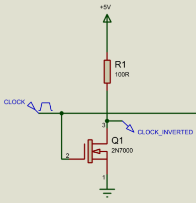
This is only really practical for higher supply voltages however, as the gate threshold voltage of a typical N-MOSFET is around 2.1V, so we will switch to a +5V supply at this point.
We connect the inverted clock to the negative of the Stage 2 capacitor:
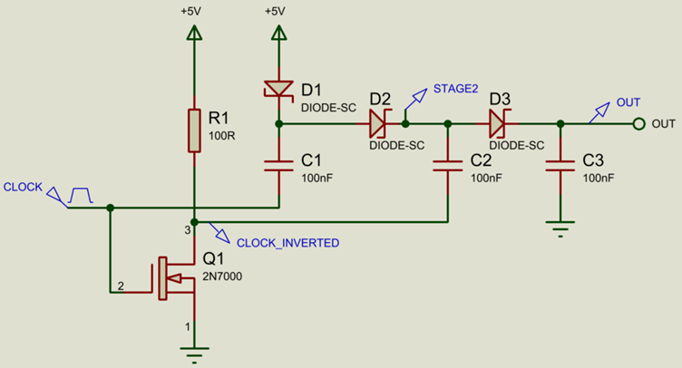
Let’s analyse how this works (ignoring voltage drops over the diodes / transistor for the sake of simplicity).
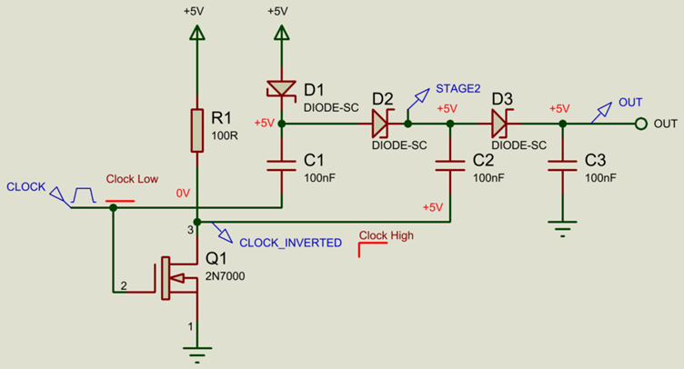
Initially the clock is low, and the Stage 1 capacitor charges to the supply voltage (+5V). The stage 2 capacitor does not charge yet as it has the supply voltage on both its positive and negative pins.
Next the clock goes high, and stage 2 gets charged to +10V like it did previously.
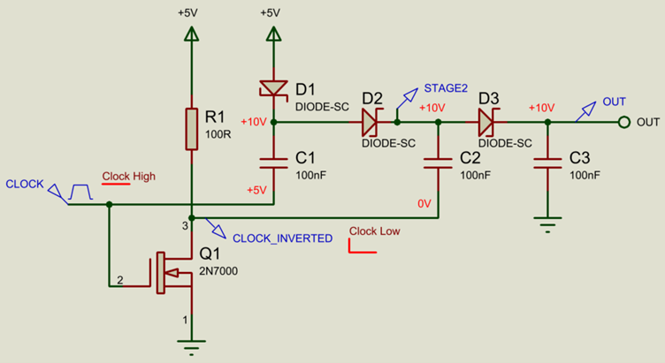
Now the clock goes low again, resulting in the inverted clock going high, and boosting the now-charged Stage 2 capacitor up to 3 x the supply voltage (+15V).

Again, due to voltage drops over the diodes and non-ideal real-world components, the output voltage is not quite +15V, but it is certainly more than double the supply voltage.

This process can be chained and scaled to produce arbitrarily high output voltages

This type of charge pump topology is called a Dickson Charge Pump.
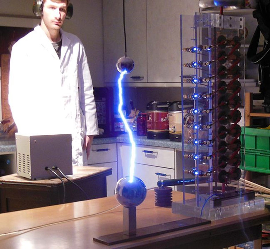
Marx Generator
Another interesting design is the Marx Generator:

In this design Spark Gaps are used as switches. Spark gaps are conductors placed a certain distance apart, which will result in electricity being conducted once the voltage across them is higher than the insulator breakdown voltage (approximately 30kV/cm for air). Once all the parallel capacitors are charged up, a chain reaction across the spark gaps is initiated by triggering the first spark gap. Using this technique, potentials of hundreds-of-thousands of volts can be generated.
Charge Pump ICs
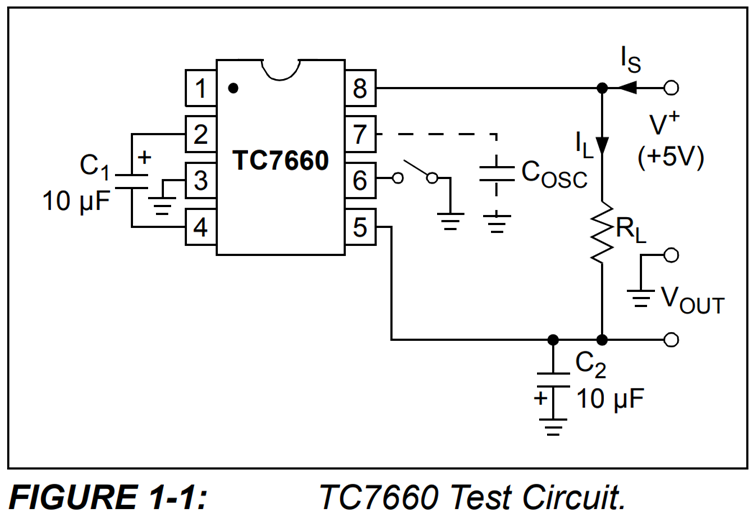
Switching our mindset back to normal electronics, it is worth mentioning that there are convenient integrated circuits (ICs) available which can ease the process of adding a charge pump to a design – requiring as little as only a supply voltage and two capacitors – such as the industry standard TC7660.
More advanced Charge Pump ICs are also available, and these can output relatively precise regulated voltages by carefully controlling the clock driving the charge pump while carefully monitoring the output voltage.
In summary, Charge Pumps offer an interesting and compact low-cost option for voltage boosting or inverting where high-current output is not required.
A demo copy of Proteus is required to open the .pdsprj file.
This article is part of a series on power conversion. Read on for a primer on boost converters and buck converters.
All content Copyright Labcenter Electronics Ltd. 2026. Please acknowledge Labcenter copyright on any translation and provide a link to the source content on www.labcenter.com with any usage.Get our articles in your inbox
Never miss a blog article with our mailchimp emails
Advanced Simulation
Learn more about our built in graphing and advanced simulation features. Harness the mixed-mode simulation engine in Proteus to quickly test your analog or digital circuitry directly on the schematic.
 Ask An Expert
Have a Question? Ask one of Labcenters' expert technical team directly.
