Testpoints can be used on the PCB in many different ways, ranging from sporadic coverage for calibration and monitoring where it's deemed necessary, to more rigorous coverage for bed of nails or flying probe testing. Proteus allows you to work with testpoints in the way which best suits your design. You can simply place and designate testpoints as needed or set up a testpoint coverage strategy and the work to ensure compliance.
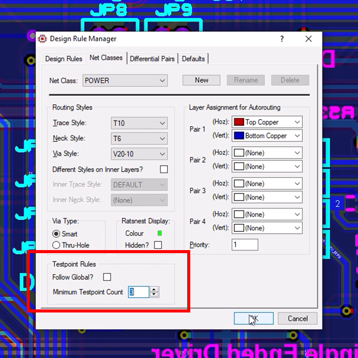
- Set minimum numbers on a net class basis.
- Define clearances, board sides and other rules.
- Either place and wire or designate existing pads/vias.
- Use the live coverage monitor to work towards compliance.
- Dedicated testpoint report and output plot.

Specifying Testpoints
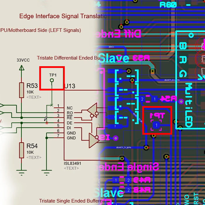
A testpoint can be either a dedicated pad or it can be an existing pad/via already on the layout. Where it is a dedicated pad the process starts on the schematic with the placement of a testpoint terminal. This results in a single pad testpoint part appearing in the parts bin for placing and wiring on the layout in the usual way. Alternatively, component pads or vias can be designated as testpoints directly on the layout via the right click context menu. Placement and sizing rules are enforced by the software in either case.

Testpoint Rules
The location of testpoints on the layout - whether placed or designated - is governed by three basic rules found on the Defaults tab of the Design Rule Manager. These settings are global to the board.
1) Testpoint Access: Determines whether testpoints must be on a particular side of the board (e.g bottom for bed of nails) or whether is access is possible from either side of the board.
2) Minimum Dimension of Pad Shape: Determines the minimum size of pad shape required for the testpoints.
3) Minimum Distance between Testpoints: This distance is governed by the pitch limitations of ICT probes and so should be set in consultation with testing to ensure access.

Testpoint Strategy
If you decide to use testpoints formally in your project then ensuring adequate coverage is important. This could be as simple as making sure there are at least two testpoints per net for flying probes or it could be something like ensuring that each power net has testpoints (or both).In Proteus you can specify testpoint requirements globally or on a net class basis or a combination of both with net class settings overriding global default settings. Both placed and designated testpoints will contribute to any testpoint requirements that are set up.

Testpoint Compliance
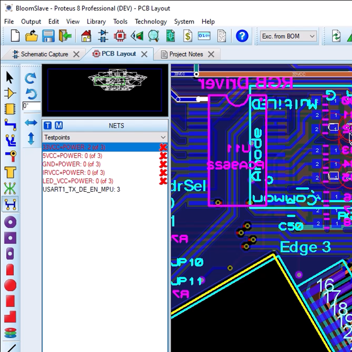
So, now you've set up your testpoint strategy and it turns out there's a couple dozen nets needing at least 2 testpoints each. Using the testpoint filter in connectivity highlights mode turns the parts bin into a live testpoint monitor. Non-compliant nets will be highlighted for attention and a double click will tag the net on the layout to make it easy for you to designate pads/vias as testpoints. You can then move on to the next net needing attention and work through until your design is fully compliant.

Reporting and Output
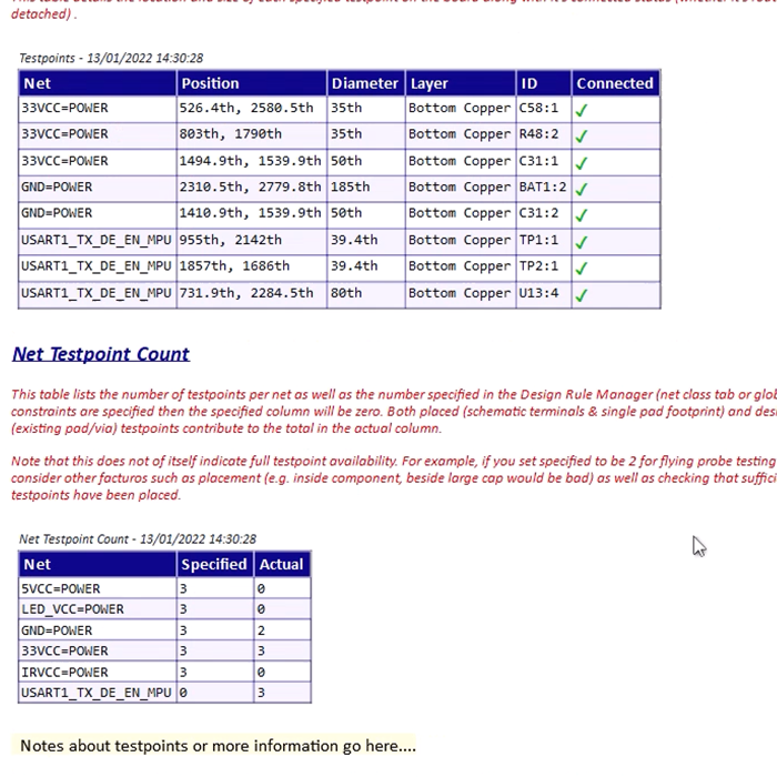
Project Notes includes a dedicated testpoint report which by default contains a graphic showing the location of each testpoint on the board along with some tabular data on net compliance and testpoint co-ordinates.
Find out more on the reporting page.
A testpoint information file can be generated which is simple CSV file listing pads which are designated as testpoints on the layout. The X, Y value is the centre of drill hole or pad origin relative to the Output Origin. Vias are only listed if they are exposed through the solder resist. The standard Gerber X2 output also identifies appropriate pads/vias as TestPads.