Designing a great product is one thing; designing a great product which can be manufactured efficiently at scale is another. As production volumes increase, the “machine which builds the machine” becomes more important, and building that machine can require much more engineering than the actual product itself. Economies of scale invariably mean automating production as much as possible, and Design for Manufacture is essential. For testing and quality assurance of both bare and assembled PCBs, it is usually necessary to include Testpoints on the board.
Testpoints on Bare Boards
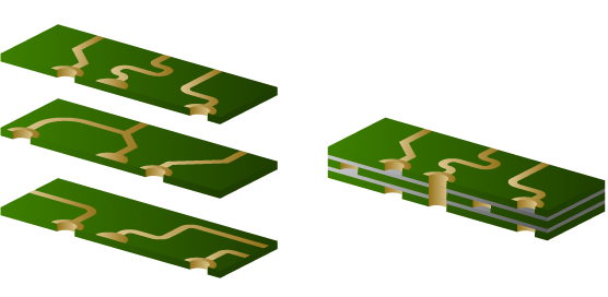
Testpoints are pads on the PCB where a signal or power net is exposed, and can be connected to by an external probe. Bare PCBs are usually tested for short- and open-circuits using the component pads themselves, and this is usually done with a “flying probe” tester. Flying Probe testers have 2 or more heads which can move around, similar to a pick and place machine, with spring-loaded needle-like probes on the ends. These probes are rapidly positioned in quick succession to contact each pad on the PCB and measure for both continuity on the same net as well as short-circuit to adjacent nets. If any problems are found, which does occur from time to time in PCB manufacture, then the board is rejected.
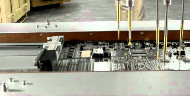 Flying probe machine on testpoints.
Testpoints on Assembled Boards
For assembled boards a number of test and QA strategies are used. Automatic Optical Inspection (AOI) machines can check that components are placed correctly and that the visible solder joints look good. If components have polarity and/or value markings on them then AOI can be used to check these as well. Automatic X-Ray Inspection (AXI) machines can be used to check components where the pins are not visible, such as with Ball-Grid-Array (BGA) chips; they can also be used to check for solder-bridges under components such as QFNs, and for voids in the solder.
Flying probe testers can also be used at this stage to measure component values (resistance, capacitance, inductance) as well as signal integrity and even LED operation and component polarity (using optical sensors on the flying probe heads). It can often be necessary to have dedicated testpoints on boards once they have been assembled, since pads may be buried under components or otherwise inaccessbile. For maximum automation at volume production, customised test jigs can be produced which not only perform measurements of the boards, but can also carry out more advanced functions such as programming of ICs and testing of communication protocols; these jigs generally use a “bed of nails” setup where dedicated spring-loaded pins are positioned at specific locations, matching the test-points.
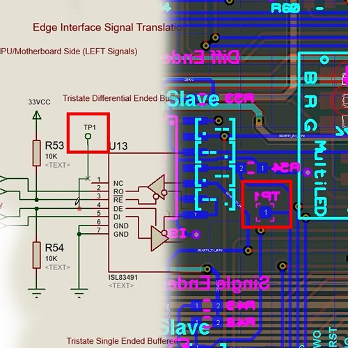
Testpoints in Proteus
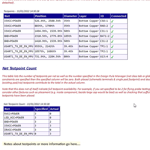
Proteus caters for both dedicated testpoint pads, specified at the schematic level, as well as assignment of component pads as testpoints. Reports can be generated and exported containing the testpoint data, and design rules can be specified such as the minimum dimensions for a testpoint pad as well as the minimum distance between testpoints.
Watch a tutorial video showing testpoint workflow here:
All content Copyright Labcenter Electronics Ltd. 2026. Please acknowledge Labcenter copyright on any translation and provide a link to the source content on www.labcenter.com with any usage.Get our articles in your inbox
Never miss a blog article with our mailchimp emails