This article shows a design process for a simple four stage BJT Amplifier based on the popular silicon 2N3904 NPN transistor. There are several advantages with multistage amplifiers, notably achieving high gain with good frequency response and low level distortion. The amplifier we are going to design is a simple cascade connection where four identical stages are connected by RC coupling. In other words we are connecting each stage by using a capacitor in series between the output of the previous stage with the input of the next one. This approach is fine if, as in this case, we don’t require the DC amplifier response.
The total gain is calculated as the product of each gain of any individual stage:
Gain = A1 x A2 x A3 x A4
However, the value of each stage gain must consider the loading effect. This is the effect of the input impedance of the next stage against the gain of the previous one. In order to get the input impedance high enough we will set a collector current IC as low as possible; 1mA will be sufficient
General Specification
We need an amplifier with at total Gain greater than 46dB, (Gain > 200), and a frequency response from less than 10Hz up to 1MHz @ -3dB. We will supply this amplifier with a 12Vdc power supply. We're going to use the popular 2N3904 NPN BJT. The 2N3904 is an epitaxial planar NPN, general purpose transistor for small signals and switching application. For our design we will use the 2N3904 in the linear region as an amplifier.
The 2N3904 Static Characteristic Curves
We can use DC Transfer Curve Analysis (available in Proteus and other SPICE tools) to help us to characterize the 2N3904 in order to find the working point in steady state condition. We can arrange a schematic file like this
A demo copy of Proteus is required to open the .pdsprj file.
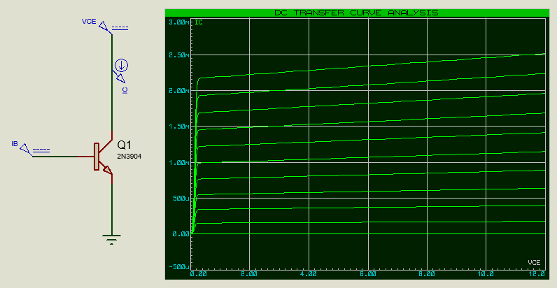 Transfer curves for 2N3904.
The transfer curve analysis window should be maximized (right click context menu) to allow us to choose the working point in the steady state condition. We're looking to see the Collector current IC value and the bias Base current IB at the most appropriate value of the Collector/Emitter Voltage VCE.
In order to get the max output voltage swing we have to choose VCE as VCC/2 or 6Vdc. On the maximized transfer curve analysis we will set the cursor on the graph area to VCE=6.00 and then look for the IB curve that sets the IC current as close as possible to 1mA value. The IB curve that satisfies this condition is 7.50µA, to which corresponds an IC current or 1.07mA. This gives us all the values we need to carry on with our design.
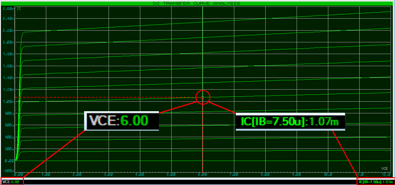 Finding Max Output Voltage Swing.
Doing the Math
We have now the following work point in steady state conditions:
VCE = 6.00Vdc ; IC = 1.07mA @ IB = 7.50µA
We set up a skeleton stage one circuit and add some current and voltage probes that will be useful for us to check all the bias values once we've calculated the resistor values of the amplifier stage.
To get these resistor values we calculate as:
R3 = VCE/IC = VCC/2IC = 12V/(2 x 1.07mA) = 5607Ω. We will approximate 5.6kΩ
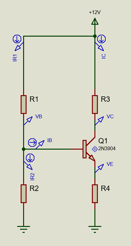
- Amplifier Stage with no resistor values yet.
The current through the bias partition resistors R1 and R2 must be much more that 10 times of the base current (IB=7.50µA). We may conveniently set this current to be 100µA and VB=1.7V (Base voltage to ground). So we have:
R1 = (VCC-VB)/IR1 = (12-1.7)V/100µA = 103000Ω. We will approximate 100kΩ
R2 = VB/(IR1-IB) = 1.7V/(100-7.5)µA = 18378Ω. We will approximate 18kΩ
Now, considering the base to emitter forward voltage VF= 0.7V and IE≅IC we will get:
R4 = (VB-VF)/IC = (1.7-0.7)V/1mA = 1000Ω or 1kΩ.
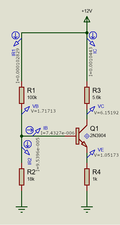
- Checking Bias Currents with resistor values plugged in.
Finally we can now assign the component values in the stage one circuit above to check if the bias currents and voltages comply with our calculations. In Proteus we can do this quickly in real time simulation mode by simply pressing the play button at the bottom of the schematic area. As we can see all bias values in steady state condition are satisfied with very good approximation. So, now we have the brick we need to build our multistage amplifier. The next step is to figure out the gain.
A demo copy of Proteus is required to open the .pdsprj file.
Predicting the Stage Gain
With resistive components in place we can compute the voltage Gain of a stage alone (not loaded) or followed by an identical stage. We can approximate the Gain by:
G ≅ -R3/R4 = -5.6kΩ/1.0kΩ = -5.6 or 20 x log(5.6) = 14.96dB
However when connecting this stage in series, the input impedance of the next stage will affect on the gain of the previous one and so to the overall gain. As such, we may reasonably approximate that the input impedance is due substantially to the collector resistance, R3, in parallel to the input impedance Ri of the next stage. We can use another graphics analysis method to evaluate the input impedance as shown below.
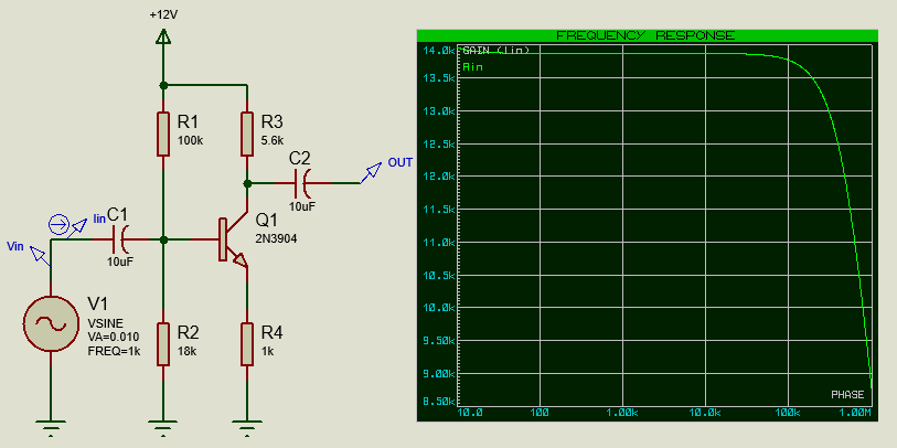 Test jig with Voltage Generator to calculate Input Impedance .
A demo copy of Proteus is required to open the .pdsprj file.
The trick to getting the the input resistance plotted on the graph is to use what's called a trace expression. This allows us to plot the result of a formula based on probes on the circuit, in this case making use of the voltage and current probes to plot resistance.
Simulating the graph analysis and maximizing it we can find that input resistance is 13.9kΩ. Now we can compute the overall gain of each stage loaded by the previous one. We call RL the loaded collector resistance; this will be the parallel of R3 and Ri. Now the loaded G will become:
GLoaded = -RL/R4 = -3.99 or 20 x log(3.99) = 12.0dB
The overall gain of a 4-stages amplifier, the which last stage is loaded by 100kΩimpedance, would be:
Gain = A1 x A2 x A3 x A4 = 3.99 x 3.99 x 3.99 x 5.3 or 20 x log (336.6) = 50.3dB
The last stage loaded resistor is the parallel of R3 and 100kΩ resulting in 5.3kΩ
The Multi Stage Amplifier
Let's now look at our multi-stage amplifier and see well it conforms to expectations. The circuit is basically a block copy of the single stage we've been working with but for convenience it's provided for download via the link below.
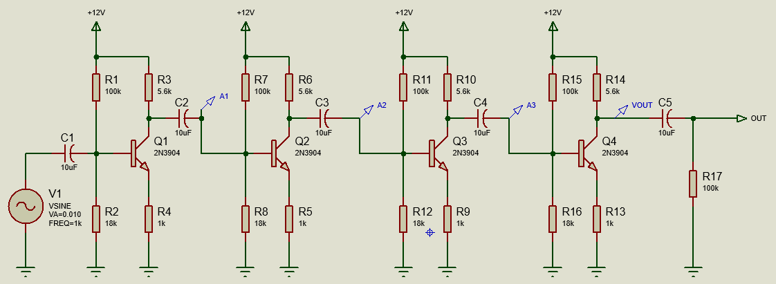 The Multi Stage Amplifier Circuit.
A demo copy of Proteus is required to open the .pdsprj file.
Graph Based Simulation
With a graph based simulation you run the simulation for a period of time and then analyse the results. We can do this in Proteus from the right click context menu over a graph. After running both graphs the results should look like the following.
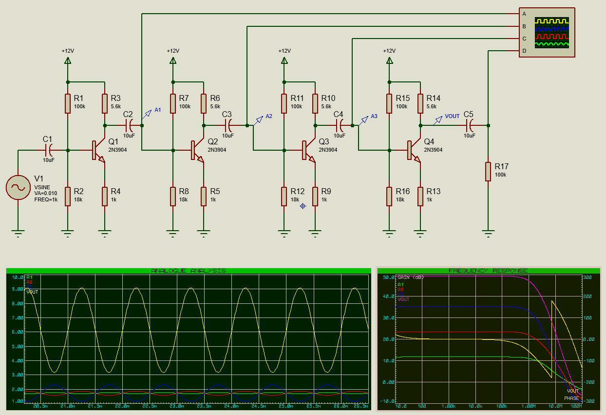 Multi Stage Amplifier Circuit Graph Results.
Graphs can be maximised via the right click context menu. Analysing the frequency response then we note an overall gain of 49.4dB or:
GVout/Vin = 1049.4dB/20 = 295
We can also see that the bandwidth at the -3dB point is 1.21MHz which also satisfies our initial specification. As a slightly picky point of clarity it's noticeable that the simulated gain value is a little lower than the overall gain we predicted with our calculations. This is because of the (very reasonable) approximation of the gain as:
GLoaded = -RL/R4
Such approximations are still acceptable as the main goal is not detailed analysis of a BJT common emitter configuration. Moreover not all datasheets report hybrid parameters and, finally, we wanted to keep things as simple as possible. A more correct gain and more accurate result would be described by:
GLoaded = - hfeRL/(hie + (1+hfe)R4
Real Time Simulation
For a bit of fun we can also run a real time simulation (via the play button) and we should see the same waveforms on the virtual scope and we would do using a real 4 channel oscilloscope.
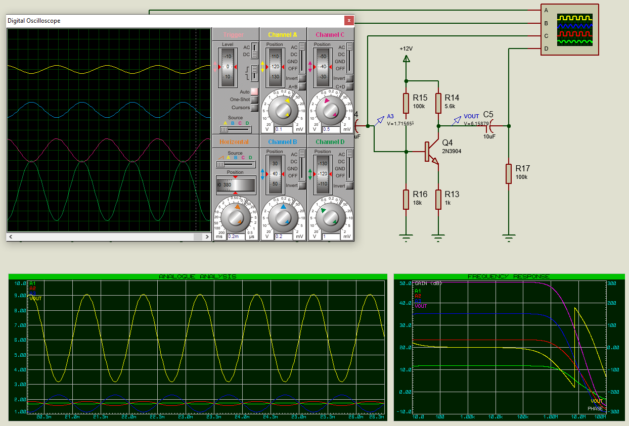 Multi Stage Amplifier Circuit Graph Results.
Conclusion
We have seen a simple example of a Multistage amplifier based on an active silicon device and how SPICE simulation in software like Proteus can simplify and aid the design of such amplifiers. This is accomplished by using tools such as Transfer Curve analysis to characterize the active devices and by the use of voltage and current probes to measure in real time the voltage and current biases in the circuits steady state condition. Finally, we've used trace expressions in Proteus to evaluate the input impedance of an amplifier stage. Hopefully this article shows how building expertise with using simulation graphs can prove to be a powerful tool for the professional designer.
All content Copyright Labcenter Electronics Ltd. 2026. Please acknowledge Labcenter copyright on any translation and provide a link to the source content on www.labcenter.com with any usage.Get our articles in your inbox
Never miss a blog article with our mailchimp emails
Advanced Simulation
Learn more about our built in graphing and advanced simulation features. Harness the mixed-mode simulation engine in Proteus to quickly test your analog or digital circuitry directly on the schematic.
 Ask An Expert
Have a Question? Ask one of Labcenters' expert technical team directly.