Regardless of which tool you use to design your PCBs you will almost certainly be able to launch and view the board in 3D. Surprisingly often, this is dismissed as being a pre-sales tool that looks good rather than a genuinely useful feature for the engineer. In this post we’ll look at the top three uses for the 3D Viewer in the Proteus Design Suite and assume the results would be similar across the industry.
3) Height Clearance
You first set a height clearance on top and bottom of the board that corresponds to the space from the mounting position to the edges of the casing. Then, you turn on the height bounds view which produces a translucent block around the board at these dimensions. While an approximation it’s a very quick and easy way to visualize where problems might lie ahead in the case design.
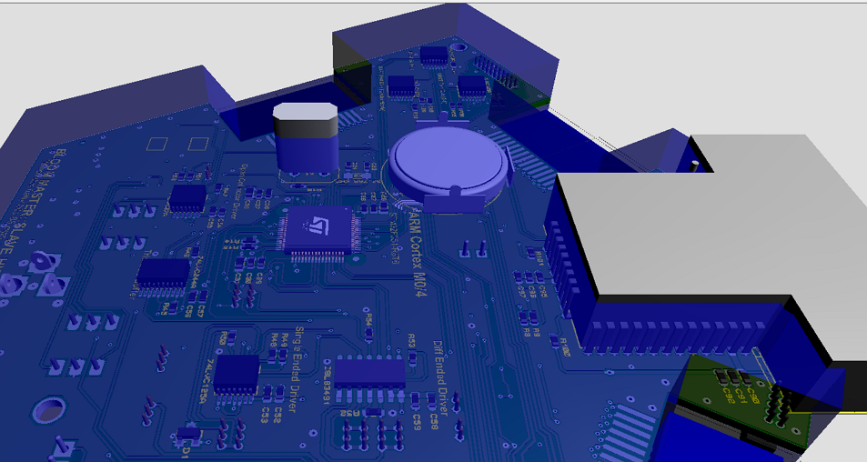 Height bounds enabled in the Proteus 3D Viewer with a clearly extruding crystal.
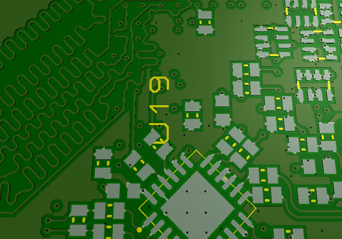
2) Bare board Inspection
Looking at the 3D View of the board with the components removed is really helpful. It’s something we’re used to seeing in real life and is great for inspecting solder mask openings. It’s especially useful in high density areas of a board where you can zoom in and look for possible issues with component placement or via positions.
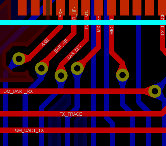
 Partial view of the underside of a board in bareboard view.
1) MCAD Output
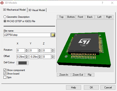
For transfer to modern MCAD the standard export from the PCB Design Software package is a STEP/IGES assembly. This means that all of the constituent parts of the layout need to have an accompanying STEP/IGES file to correctly represent their dimensions.
Fortunately, this is now such an industry standard that most library part vendors will include a STEP file with all of their parts and there are also numerous web resources with STEP file libraries. Adding a STEP file to a footprint is in many cases an automatic process and if it does need to be done manually is really simple (see image opposite).
The end result is not only that your 3D View is a more accurate representation of the real board but that you can export it with a mouse click directly to MCAD tools like Solidworks or Autodesk.
Summary
The 3D Viewer is a great place to inspect your work, spot problems or improve your layout. So the next time you get towards the end of your layout work take a few minutes and explore whether your 3D Visualization tool can help you.
To learn more about 3D Visualization in Proteus watch the tutorial video below
All content Copyright Labcenter Electronics Ltd. 2026. Please acknowledge Labcenter copyright on any translation and provide a link to the source content on www.labcenter.com with any usage.Get our articles in your inbox
Never miss a blog article with our mailchimp emails