Introduction to Package Types
When an Integrated Circuit is cut from the Silicon Wafer, it can be packaged in a number of different ways, including:
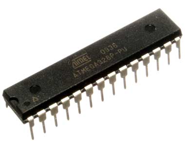 Dual Inline Package (DIP).
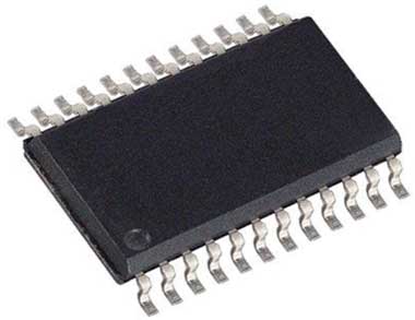 Small Outline Integrated Circuit (SOIC).
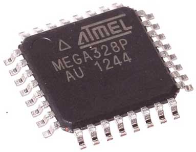 Thin Quad Flat Pack (TQFP).
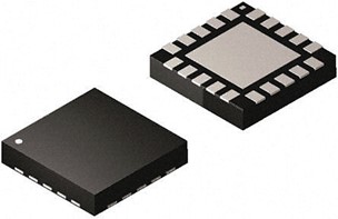 Quad Flat No-Leads (QFN).
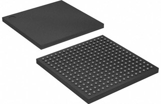 Ball Grid Array (BGA).
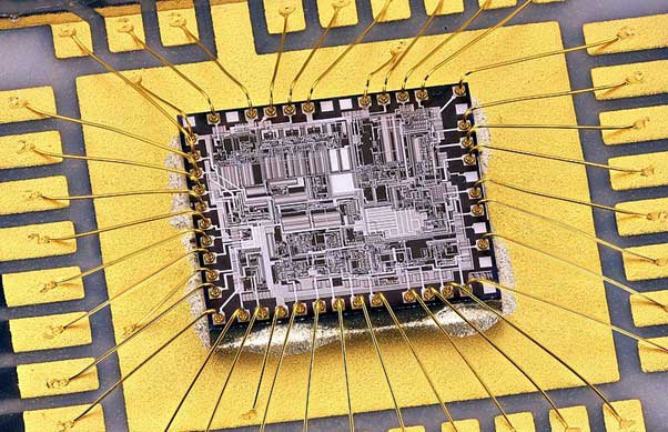
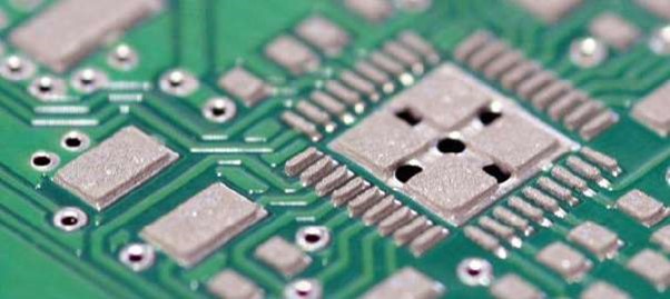
Inside the different plastic packages, connections are made from the Silicon IC to the Package Pins using a technique called Wire Bonding.
DIP packages are larger and easier to hand-solder (better for hobbyists), wheras BGA packages cannot be hand-soldered and require special equipment for assembly onto a PCB.
BGA packages have the highest pin density, meaning that they occupy the smallest space on the PCB which is essential for most modern high-end electronic products (such as smartphones). Having such high-density packages however means that special techniques are needed to route all the signals out on the PCB.
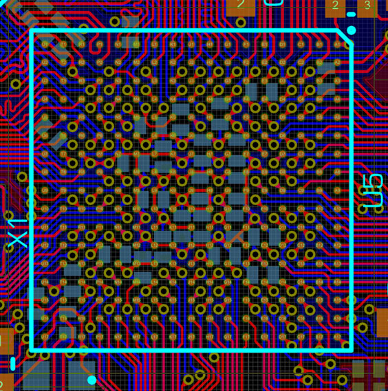
The following are some general tips about routing BGA chips during PCB Design.
Design Rules
The first step, before even starting PCB layout, is to decide on the design rules.
- How many layers will the board have?
- What is the minimum track width?
- What is the minimum track spacing?
- What is the minimum via size (minumum drill diameter and minimum annular ring)?
In general, the more layers and the tighter the feature tolerances the easier it will be to route the board. More layers and tighter tolerances will also generally make the board more expensive however (and slower to manufacture).
Product Volume
One of the decision factors is the anticipated product volumes – how many of these boards are expected be made? For high volume products it may be worthwhile to put the extra effort into carefully routing using as few layers as possible in order to shave down the per-PCB cost, whereas for low volume products the labour-cost of spending-additional-time-routing-to-less-layers is not justifiable.
It is also necessary to check what your PCB manufacturer’s capabilities are, and whether they can actually even produce a board with the specifications you are designing to – i.e. what their minimum track width, track spacing, drill size and annular ring specifications are (as well as the maximum number of board layers is which they can produce).
Impedance Requirements
Another factor is impedance requirements and whether any (many) of the tracks require specific impedances – since the track widths, track spacings and layer stackup will determine the track impedance. Also, it goes without saying that some of the inner layers of the board will be power-supply reference planes (for constant impendance); please check our high-speed design articles for more information if you are not already familiar with this.
Some BGAs – such as micro-processor units (MPUs) – feature multiple power domains, and the power-plane(s) on the inner layer(s) of the board will normally be broken up into different sections depending on the power connections used in that particular area of the chip. For example the DDR memory may work at a particular voltage and will have a power-place spanning the DDR chip as well as the DDR section of the MPU, whilst the SD/eMMC section will work at a different voltage and have its own power-place spanning that memory and that section of the MPU.
Having the correct power-plane under the relevant pins is important for impedance-matching, but also makes routing those pins easy as all they require is a via down to the power plane (rather than a track routed outside of the BGA area).
Part Documentation
Sometimes the IC datasheet will have recommendations regarding some of the design rules, such as this excerpt from the ST Microelectronics STM32MP1 application note on getting started with the hardware design for that processor:
In general it is always essentially mandatory to check the part documentation for any design requirements or recommendations. There may also be specific design constraints for routing certain sections of the design, such as impedance and spacing requirements on the DDR connections.
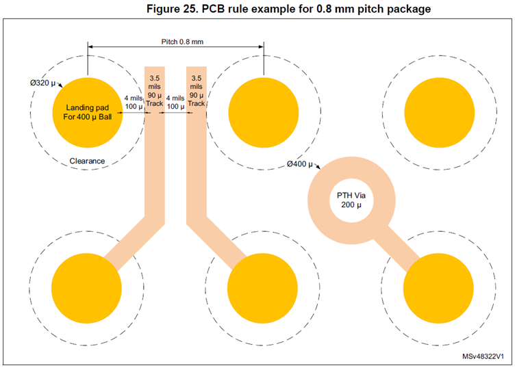
When pulling in PCB Footprints from libraries then it is worth checking the BGA landing pad size of the imported parts – as a general rule these should be 80% of the diameter of the BGA ball, however they are not always set as such on imported footprints.
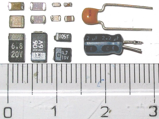
BGA chips will almost always require decoupling capacitors and possibly calibration resistors placed close to the chip (usually directly underneath it), and so deciding on the package size for these is also an important step which should be done in advance. Again, the smaller the package size the easier routing will be, but the more advanced (and therefore potentially more expensive) the equipment and processes required for PCB assembly.
Another source to check when deciding on design rules is the reference design board(s) for the chip. Regardless of the PCB Design softare used, manufacturers will usually provide the board Gerber files which can be opened and inspected using Gerber Viewer software such as ViewMate. Layer count, track widths, track spacings, and via dimensions can all be checked.
Via Options
Another potential design decision is whether blind and/or buried vias will be used, which are again more expensive but again also make higher-density designs easier (or even possible). Via-in-pad technologies are another technique which can be used to increase density, however again at a higher cost.

Watch how to deal with resin filled vias in Proteus here
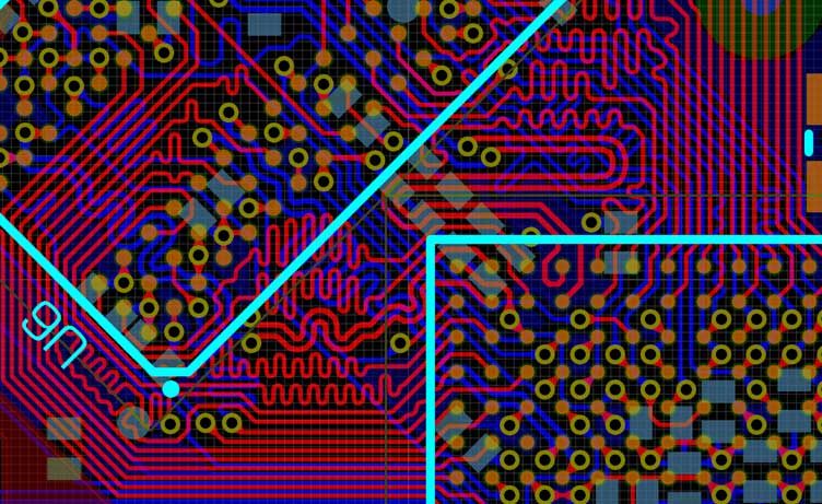
Placing Routes
Another source to check when deciding on design rules is the reference design board(s) for the chip. Regardless of the PCB Design softare used, manufacturers will usually provide the board Gerber files which can be opened and inspected using Gerber Viewer software such as ViewMate. Layer count, track widths, track spacings, and via dimensions can all be checked.
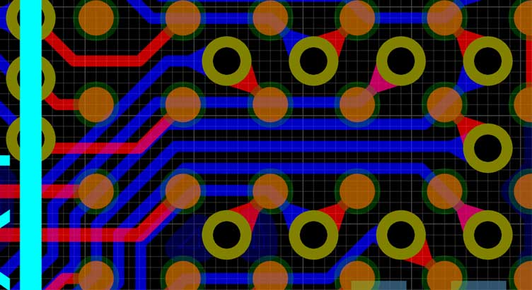
Some BGAs have selectively populated balls, where some ball positions on the BGA are not used in order to create escape channels for routing tracks through.
Removing the non-functional pads on inner layer vias can help to free up more room for routing (when using 6-layer+ boards).
Learn about non-functional pads in Proteus here
Vias are typically arrayed in the dog bone fashion.
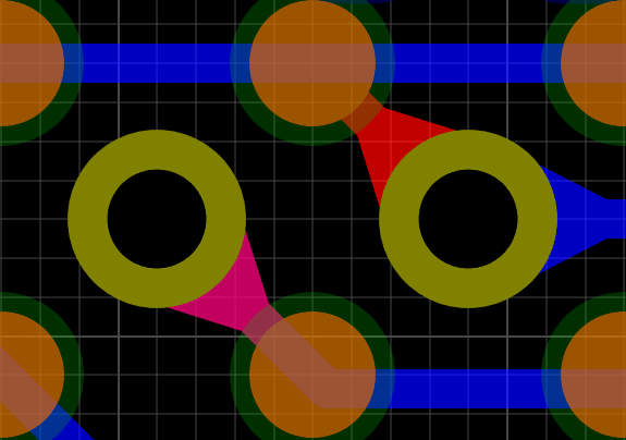
One technique for increasing the density of tracks escaped from the inner rows can be to arrange the vias in such a way as to create a channel where multiple tracks can be routed out in close proximity:
As a final tip, it can sometimes be helpful not to place adjoining chips (such as MPU and DDR) too close to each other in order to leave sufficient space for length-matching serpentines which often take more space that you might think.
 All content Copyright Labcenter Electronics Ltd. 2026. Please acknowledge Labcenter copyright on any translation and provide a link to the source content on www.labcenter.com with any usage.
Get our articles in your inbox
Never miss a blog article with our mailchimp emails
.jpg)