Via stitching on the PCB is where a large number of vias are used to connect copper areas on different layers together. Via shielding (sometimes called a picket fence) is where one or two rows of vias connect copper pour together at the perimeter of some tracks or the copper pour areas. There are many different views on when and how to use stitching / shielding vias on your PCB, some of which we’ll summarize in this post.
Constant Ground
Probably the most common use for stitching planes with vias is to ensure short return paths for signals or to help maintain a constant ground. As soon as any current starts to flow it will cause a voltage across the copper through which it is flowing, serving to both spread the current out but also cause the ground to 'bounce' around depending on which part of the PCB is being looked at. Via stitching can be an effective and low-effort way to more tightly couple ground across the PCB.
Thermal Management
On some PCBs stitching vias can be helpful in distributing heat. A PCB is more conductive horizontally (across the layer) than it is vertically (through the board). If tracking is only on the outer layers then a lot of the heat is carried sideways and the core may well be cooler than the traces. Stitching this construction with vias produces quite a bit more through-plane conductivity which carries and dissipates heat to the core, reducing overall temperatures. This advantage would go away of course if the whole board is used to carry current and therefore there is no spot which is cooler for the heat to spread out into.
Crosstalk
Stitching copper can also be used to reduce capacitive coupling between signals. Think of two adjacent traces on the board as the terminals of a capacitor with the gap between them as the dielectric. A wider gap means less capacitance and less crosstalk. Stitched copper between tracks therefore has the same effect as a smaller gap (more crosstalk!) unless the copper is well grounded. It’s important therefore to consider whether the stitched copper is effectively grounded at the frequency of interest. In this role, stitching vias tend to be used on high impedance, analog circuitry (ADCs, SMPS, etc.) where there is a lack of solid reference planes.
EMI
Stitching of copper around tracks at high frequency is done for different reasons entirely. The goal here is to fence in electromagnetic waves radiating from these tracks. Sadly, insulators of current – including the FR4 dielectric core of the PCB - are good conductors of electromagnetic waves. When signal frequencies get high enough that the wavelengths are of similar size to copper features on the PCB the two ground planes become helpful waveguides, bouncing electromagnetic waves between them on their way out through the side of the board. Suggested practice is therefore to stitch/shield ground planes on an RF board with vias spaced at a minimum 1/10th the wavelength of the highest frequency of interest. The point is to keep the spacing small in comparison to a wavelength in the substrate dielectric so as to make the fence appear solid to impinging waves.
Many internet resources (e.g. Via Fence Wikipedia) exist with far more detailed guidance.
Copper Balancing
Finally, stitching planes together may have advantages during board manufacture because the vias can tie otherwise unconnected copper areas (islands) to the net, allowing greater copper coverage. The result generally is that the PCB will have more balanced amounts of continuous copper on each side of the board which can help prevent warping during reflow.
Applying Stitching Vias
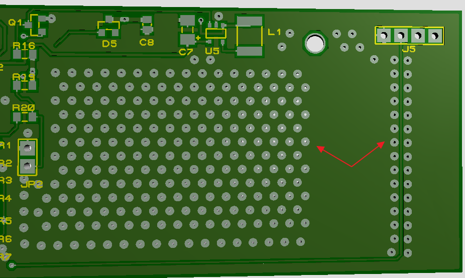
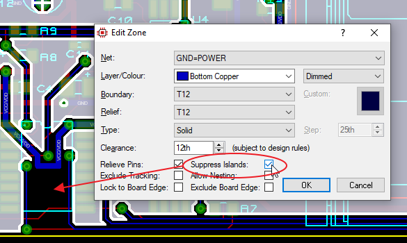
Most EDA Tools will provide some mechanism for automatically stitching two copper pours together. The first user decision is whether to include islands in the copper flood. An island is a flooded copper area which has no connection to the net on its layer but will acquire a net connection when stitched to the other copper pour. In the Proteus Design Suite, the suppress islands checkbox is used to control the copper pour when you place a power plane.
Once the flood areas on both layers are defined the user would invoke the via stitching command. Normally, a configuration dialogue will enable choice of via style and minimum clearance between vias and the software will then take care of the via placement. Once configured this will typically stitch the entire common area of the two planes.
While it sounds obvious one of the most common user mistakes is to stitch planes together too early in the layout package. A fully stitched PCB will make routing traces much harder and so, unless there is good reason, stitching should always be performed after routing is complete.
Applying Shielding Vias
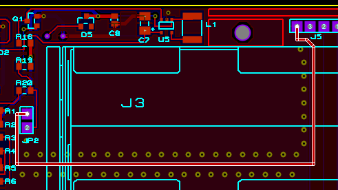
Shielding vias, sometimes called via fences or picket fences follow the same principles as stitching vias but tend to consist of a single row of perimeter vias around either tracks or the copper pour boundaries. These are almost always used to isolate areas of the board operating at different frequencies and for EMI control as discussed above.
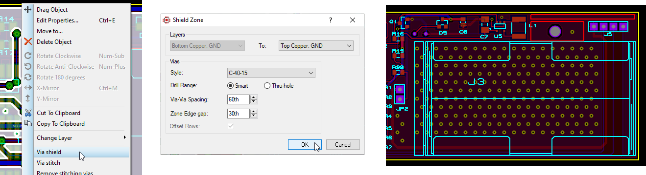
Procedurally, you would apply shielding vias in almost the same way. You can select either the track(s) to be shielded or the power plane if the vias are being applied to the copper pour perimeter. The via shielding dialogue is then launched from the context menu and configuration takes place in the same way as for via stitching.
Summary
Whether or not you need to stitch your copper pour together is a commonly debated question by PCB designers with far more talent and experience than me and the answer in any situation requires a fair amount of product specific knowledge. However, hopefully this post covers the main issues involved and gives you some ideas about how stitching planes could help your PCB design.
If you’re interested in how to use via stitching in the Proteus Design Suite a short tutorial video is linked below:
All content Copyright Labcenter Electronics Ltd. 2026. Please acknowledge Labcenter copyright on any translation and provide a link to the source content on www.labcenter.com with any usage.Get our articles in your inbox
Never miss a blog article with our mailchimp emails