Ever wondered what's involved in getting a board mass produced ? Specifically, what steps are involved in getting from the bare board PCB to the final assembled product? We'll look at a few of those steps in this article.
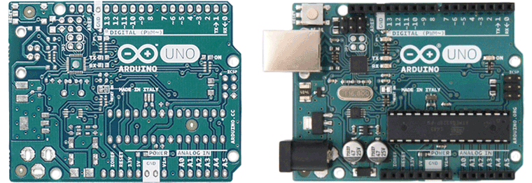 Arduino board before and after component placement.
Component Procurement
Component procurement is the process of purchasing all of the components needed to assemble the PCB. Components come is various standard packagings, designed to make automated assembly possible; for example Tape & Reel, Tube, and Tray. Standard packaging is also usually supplied with standard component quantities – for example 5000 resistors on a reel; some component distributors do however offer a reeling fee, where they will take a smaller strip of components and load them onto a reel for you (with “leading” and “trailing” empty sections of tape added, which aid in loading the reel into automated assembly equipment). “Bill of Materials” (BoM) output from your PCB Design software can be used to create a list of the components and quantities needed (Proteus has a dedicated Bill of Materials module in the software), which can easily be multiplied up in a spreadsheet for multiple boards.
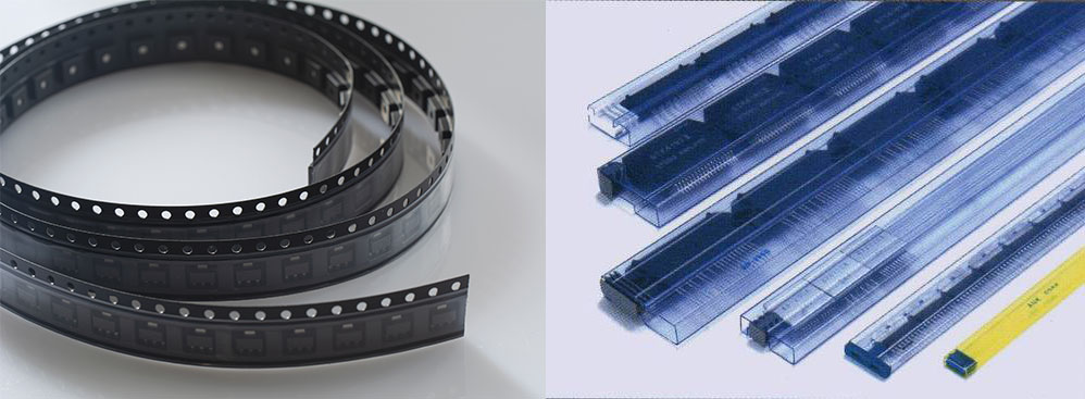 Component Tape and Tube packagings.
Machine Feeding
Components (in the standard packagings) are loaded into assembly machine “feeders”, which automatically feed components into the machine as they are used by it. Tape & Reel packaged components consist of a tape with holes for a cog wheel to pull it in on, and a plastic strip stuck on top which holds the components in place inside the strip and then gets peeled off just as the components are needed. Tubes are fed into the machine with vibration feeders, which vibrate the components along and out of the tubes. Trays are usually just opened and placed into the machine at a specific position.
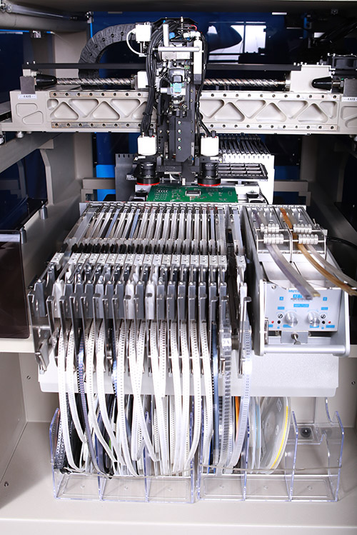 Component packaging placed in Feeder.
Machine Programming
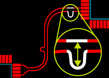
At some point, someone needs to explain to the machine which components are supposed to go where on the PCB. This is usually done with a Pick and Place file, which includes a list of the components as well as their X & Y co-ordinates on the PCB and their rotations. Pick and Place files are generated by the software which the PCB was designed in. Depending on how clever the machine is, it may also need to be told which components are in which feeders, so that it knows where to find them. Finally, the machine will also need to know the location of the fiducials on the PCB, as well as a rough location of where to start looking for them. Further considerations such as how quickly or slowly to place a component, how much force to use to pick up a component, and so on, may also need to be programmed in. Because different machines can require the Pick and Place files in different formats, Proteus includes a fully customisable Pick and Place file generation dialogue. The BoM (Bill of Materials), which we mentioned during the Component Procurement step, can also be helpful at this point. Proteus can also produce an Assembly Drawing, which is especially helpful if some or all of the Component References have not been included on the board silkscreen.
Solder Paste
Broadly speaking, electronic components come in two types – “through hole” or “surface mount”. “Through Hole” components have pins which go through holes in the PCB and are soldered typically on the opposite side; “Surface Mount” components lie on the surface of the PCB. Through hole components are mechanically stronger, however surface mount components are smaller and better suited for automated assembly. Surface mount assembly starts with applying “solder paste” to the PCB; solder paste consists of tiny balls of electronic solder suspended in a flux solution, giving the appearance of a gray paste to the naked eye. Solder is a mixture of metals with a relatively low melting point, used to bond components to a PCB with an electrically conductive connection. Solder broadly comes in two types – leaded and lead-free: Leaded solder solders more easily (at a lower temperature) and is believed to reduce the formation of “tin whiskers”, however it has been banned in many countries due to the poisonous properties of lead (tin whiskers are tiny strands of metal which can very rarely grow out of solder and result in short circuits, and have even been responsible for the failure of satellites in space). Lead-free solders do not contain lead, and are more difficult to solder due to having a higher melting point.
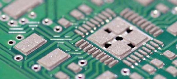 Solder Paste on PCB.
Solder paste is usually applied to a PCB using a stencil – typically a thin piece of stainless steel with holes laser-cut into it where the solder paste should go through; the solder paste stencil is placed on top of the PCB, and then a squeegee pastes the solder paste across the stencil and through the holes; when the stencil is lifted up again the solder paste remains on the board in all the right places. There are also machines which can print solder paste on using a nozzle, however the stencil method is faster and therefore better suited for volume production. The data needed to produce the stencil is usuall included in the Gerber files generated for PCB production. A reduction is typically applied so that the solder paste desposited is a little smaller than the component pads themselves. In Proteus it is possible to turn the “Paste” layers on and off in order to see exactly where there will be solder paste on the board, as well as visualise this in the 3D Visualiser. After solder paste has been applied, the board may optionally go into an automated solder paste inspection machine, which verifies that the pasting process completed successfully and with no mistakes.
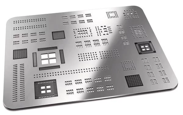 PCB Solder Paste Stencil.
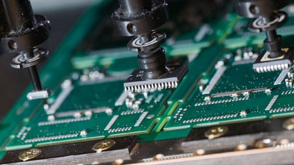
Component Placement
Next, the pasted board goes into one or more “pick and place” machines (the ones which we loaded components into and programmed earlier). These machines use vacuum nozzles to pick components out of the feeders and place them in the correct locations on the board (top machines do this faster than the eye can see!).
 Component Placement with Pick and Place Machine.
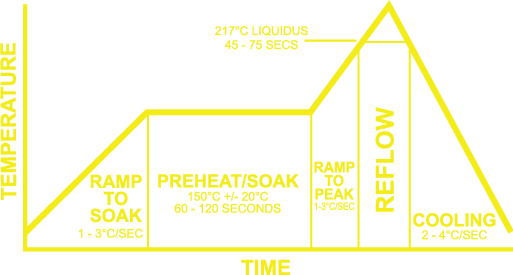
Reflow Soldering
Once all components have been correctly placed on the pasted PCB, it is time to heat everything up and melt the solder; this is typically done with a reflow oven. Reflow ovens take boards through a controlled temperature profile; first the boards are heated up to allow the PCB and components to absorb some heat (but not hot enough to melt solder), then the temperature is quickly ramped up enough to melt the solder, and then the temperature is ramped down again back to room temperature. Heating up the components and PCB first ensures that the solder will adhere properly and not result in “dry” joints.
 Reflow Solder Process.
Inspection
After reflow soldering, the boards may go into an “Automated Optical Inspection” (AOI) machine, which uses cameras to ensure that all the right components are in all the right places, and that everything soldered correctly. If an AOI is not available then visual inspection by a human is normally done.
Through-Hole
If the board contains through-hole components, then these may be added to the board in a few different ways:
- Hand Soldering, by a person with a soldering iron.
- Robotic Soldering, by a robot with a soldering iron.
- Wave Soldering
In the Wave-soldering process, through hole components are placed into/through the board and their legs trimmed to the desired length. After this they go onto the conveyor-belt of a wave soldering machine, where they are first sprayed with flux and then passed over a “wave” of molten solder which adheres to the right spots on the board (those not protected by solder-resist).
Washing
After soldering, boards may optionally be washed to remove soldering flux residues; this can improve the bonding of conformal coating in the next step.
Conformal Coating
Assembled boards can optionally be covered by “conformal coating” – a clear lacquer layer – to protect them from corrosion.
Done...
At this stage we have a completed assembled circuit board. Other steps will likely also be involved, such as microcontroller programming, quality assurance testing, placing inside an enclosure, and so on, however in this article we have covered the main points relating to the manufacture of the assembled PCB itself.
If you're looking for a CAD tool that can help you design and layout quality PCB boards read on here : Proteus PCB Design tools.
All content Copyright Labcenter Electronics Ltd. 2026. Please acknowledge Labcenter copyright on any translation and provide a link to the source content on www.labcenter.com with any usage.Get our articles in your inbox
Never miss a blog article with our mailchimp emails