If, like me, you come from a firmware background you probably prefer to think of digital electronics as on and off or high and low; those on and off signals travelling instantaneously and reliably through the electrical circuitry. Binary, instant and reliable. Certainly from a programmer’s viewpoint, this level of abstraction is assumed at the software level!
Working with faster and faster electronics however, as clock speeds move from the MHz to the GHz, it becomes obvious that things are just not that simple. In this article we will look at some of the factors which make high-speed design more complex, as well as some of the techniques used to address them.
Slew Rate
Let's start with slew rate. We need to understand that there is no such thing as an instantaneous transition from 'off' to 'on' – the voltage has to transition from the low level (e.g. 0V) to the high level (e.g. 3.3V), passing through all the voltages inbetween, even if it does so very quickly; at some point in time during the transition it is 1.8V, and at another point in time it is 2.5V, and so on. The speed at which the voltage transitions from its low state to its high state is called the slew rate.
Speed
Electrical signals also have a speed limit – the speed of light. The speed of light is 299 792 458 m/s, which is very fast. Considering however that a 1GHz signal has a period of 1ns (1 nanosecond), light only travels at approximately 0.3 m/ns, or 30 cm/ns; meaning that over a 30cm long conductor, the first clock pulse of a 1GHz signal is only just reaching the other end of the conductor by the time the next clock pulse is being generated at the start of it.
Make that 3GHz, and the source of the clock signal is already generating the 3rd pulse by the time the 1st pulse is reaching the other end of the conductor! Thinking about that (3GHz, 30cm conductor), this means that our single 30cm conductor ‘contains’ 3 pulses, 3 high and low states, within its length. This is certainly not instantaneous on/off from one end of the conductor to the other!
 Signal Transmission can no longer be thought of as instantaneous!
Reliability
Whenever electricity travels through a conductor, it generates a magnetic field around that conductor – however small that may be. Conversely, when a magnetic field passes through a conductor, then it generates a voltage within that conductor (via the electromotive force). All of the conductors in the circuit – typically tracks on the PCB – are thus capable of both generating and receiving electromagnetic interference, which can distort the signals meant to be carried by the tracks. Each track on the PCB can also be viewed as a small radio antenna, capable of both generating and receiving radio signals, which can distort the signals meant to be carried by the tracks.
Impedance
As described under the ‘Speed’ section, our electrical signals are not instantaneous, and actually travel as waves in our conductors. In our 3GHz / 30cm trace example, there are 3 waves – peaks and troughs – within the conductor at any given time. Waves are subject to various phenomenon, the most important of which to us is “reflection”.
Let’s imagine that our conductors are like water-filled canals / channels. A wave is generated at one end of the channel, and makes its way along the channel (at close to the speed of light) to the other end. Imagine that our channel was 100cm wide, but at a certain point it was suddenly narrowed to being only 1cm wide – when our wave reached the suddenly narrowed section (essentially a wall with a small gap in it), most of the wave would bounce off the narrowed section (wall) and back towards the transmitter.
 Wave reflection due to width change.
If there were multiple narrowed sections within the canal / channel, then there would be multiple reflections bouncing around, interfering with the signal. Most of the energy of the signal would also not be reaching the receiver (at least not at the correct time). It is therefore important that the width/height of the channel stay as constant as possible along its length, to avoid reflections.
 Multiple changes in width degrading the signal.
In electrical terms, this is known as “impedance”, which is a function of the resistance, capacitance and inductance of the conductor. For high-speed design, we therefore want to try and keep the impedance of our tracks as consistent as possible along their length. Another thing to consider, especially in bus topologies, is that we want to ‘stop’ the wave at the receiver and not have it bounce back again – this is usually done with a terminating resistor, which absorbs the energy of the wave at the end of the bus (such as in RS485).
Signal Integrity
So now we know what all of these physical effects are and that they can (will!) act to mess up our signal when frequencies are high. We need to stop looking at our digital communications as being binary, instant and reliable, and start taking slew, speed, magnetic interference, and impedance into consideration when designing our circuitry.
Thinking about signal integrity during PCB design just means taking account of all of these factors and laying out the board with countermeasures in place to make sure our receivers get the right message. Here's a short intro to a couple of the more common techniques used in high speed PCB design.
Length Matching Tracks
When we have communications signals which use more than one line, such as ‘clock’ and ‘data’ – perhaps even a parallel bus with 8 or more data lines – then we have to make sure that the signals all arrive at the receiver at the same time. Once we understand that electrical signals do not travel instantaneously, then we can understand that if multiple signals travel over different lengths of tracks then they will arrive at the receiver at different times (even though they were transmitted at exactly the same time).
 Uneven track lengths can lead to incorrect signals at the receiver.
Consider a communications scheme with 1 clock line (C) and 2 data lines (A and B); if the length of data line B is considerably longer than the length of data line A, then the signal from clock pulse #1 on the B line could potentially arrive at the receiver at the same time as the signal from clock pulse #2 on the A line is arriving there, completely distorting and corrupting the communications.
 Tracks A and B have different lengths.
Another way to visualise this is to imagine runners on two different tracks. Each runner can only carry half a message and the message is re-assembled at the finish line. If the runners travel at the same speed, and the tracks are the same length, then they each arrive at the destination at the same time and the receiver can reassemble the document correctly.
However, if the tracks are not the same length then our runners don't arrive at the same time and the document can't easily be re-assembled. It is therefore really important that our track lengths in multi-line communication signals are made to be the same – this is known as 'track-length matching' or 'net tuning'.
 We deliberately add length to track A so that distance from source to receiver is the same as track B.
Differential Pairs
‘Differential pairs’ is a communication technology which is highly immune to electromagnetic interference (and therefore reliable). Perhaps the most common and easily recognisable implementation of this is USB. Another technology implementing differential pairs is RS485. Differential pairs use a ‘push-pull’ technique over two parallel conductors – one ‘pushes’ whilst the other ‘pulls’. If one line is ‘high’, then the other must be ‘low’, and vice versa.
The signal in a differential pair is measured as the difference between the voltages on either conductor. Differential pairs are routed strictly parallel to each other, and in phase with each other. In addition to being track-length matched, the in phase requirement means that if the differential pairs round a bend – which will result in the outer track taking a longer path than the inner track – then the inner track must artifically add a little extra length to its track as soon as possible in order to get the total distance from the start/end of the parallel pair equalised again as soon as possible.

- Routing a curved Differential Pair

- Track added to keep pair in phase

- Track added to keep pair in phase
Any interference which a differential pair may encounter should affect both tracks equally, so the difference between them will stay constant and reliable. It is important to keep the tracks in phase however, so that if electromagnetic interference is experienced at one particular point in the track then it will affect the parallel signals in the same way. If the signals are out of phase, then the peak of one side of the signal may be affected whilst the trough of the other side of the signal is affected.
 Interference effects both signal lines equally provided they are in phase.
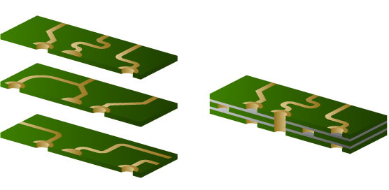
Via Stitching and Shielding
As the name implies, via shielding is a technique to ‘shield’ tracks from both generating and receiving electromagnetic interference. ‘Power Planes’ (also known as ‘Ground Planes’ or ‘Copper Pours’) are placed to surround the track or tracks, on multiple PCB layers, and vias are used to then stitch those layers of power planes together, creating the effect of a ‘shield’ around the track.
 Via Shielded Diff Pair tracks
Higher slew rates, the speed at which signals transition from “high” to “low” or vice versa, generate more electromagnetic noise than lower slew rates. Slew rate itself is usually specified in a chips data sheet (sometimes configurable, such as with some microcontrollers) so is not determined by the PCB design phase, however signals with known high slew rates can be given more attention in terms of shielding.
Via stitching is used to “stitch” two power planes together. One reason for this is to provide a short “return path” for a signal, which is important for things like impedance matching.
Summary
High Speed Design takes a lot of digital engineers a little out of their comfort zone at first. Binary, instant and reliable are no longer a given for digital signalling and so we need to actively take steps to protect our signals on the PCB. Hopefully this article de-mystifies the problems a little for beginners and gives a couple of points for future research.
Meanwhile, if you're looking for a CAD tool that can help you with high speed design then why not take a closer look at Proteus PCB Design tools.
All content Copyright Labcenter Electronics Ltd. 2026. Please acknowledge Labcenter copyright on any translation and provide a link to the source content on www.labcenter.com with any usage.Get our articles in your inbox
Never miss a blog article with our mailchimp emails