When designing a 2-layer PCB there is no real need to consider the construction of the PCB at the fab house. However, when the number of layers on the board is four or more the stackup of the PCB is an important factor. The chosen layer stackup defines the available drill ranges for vias and can also impact on the EMC performance of the product. This post discusses common manufacturing processes for multi-layer PCBs and what information you should specify in your EDA tool to help with fabrication.
Constructing a multi-layer PCB
Before looking at how layer stacks are managed, it is worth a short recap of terminology and common fabrication options for PCBs.
- Pre-preg is essentially woven fibreglass coated in unset epoxy resin.
- A core is basically ready made copper-foil/pre-preg/copper-foil or copper-foil/pre-preg.
A board house will generally have double sided copper clad core in stock as a base to start from. They will drill, through-hole-plate and etch, one or more of these cores. They will then overlay the board with pre-preg, then either bond that to another core (this core could be a basic core or already have had additional layers of pre-preg and copper foil) or a foil. Multiple layers of pre-preg can be used together to make up thicker insulating layers.
This process creates a basic set of rules as to what is manufacturable using conventional processes, in particular for drilling. Let's take a closer look using a 4-layer board as an example.
4-Layer Board
With a 4-Layer board there are basically two ways to create the stack.
You can use two cores, individually drilled and plated and stuck together with pre-preg and then a final drill/plate pass:
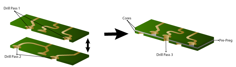
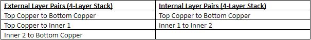
Most PCB design software, including the Proteus Design Suite, refer to this type of stackup as external layer pairs because the cores are built from the outside in.
Alternatively, you can use one core which is drilled and plated. Then a layer of prepreg/foil is placed on either side of the board, this is cured, etched, drilled, plated.
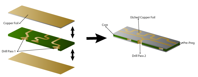
Unsurprisingly, this is normally referred to as internal layer pairs because the cores are built from the inside out.
When a multi-layer PCB is constructed a separate pass of the CNC Drilling machine is required for each drill span. This means that, having set up the layer stack there is a known legal set of drill spans which are possible. For example, in the 4-layer board discussed earlier you could have three drill spans in the case you were using two cores (external layer pairs) or two drill spans in the case you were using one core (internal layer pairs).
EDA Tool Setup
We can see from this that the layer stackup dictates available drilling ranges using standard manufacturing techniques. You cannot for example have a buried via between Inner 1 and Inner 2 if your 4-layer stack is constructed with external layer pairs. Therefore, when designing a multi-layer PCB the most important thing is to think through your required via usage and get the layer stackup configured in your EDA tool right at the beginning. This is also the place to specify the materials, thicknesses and dielectric constants for your PCB. This information is not only useful for the fab house but can also be used by your EDA tool; layer thicknesses, for example, can be used to include drill depth in length matching calculations.
Once the layer stackup is confirmed the next step is to define the via ranges you plan to use. Normally, the EDA tool can help you with this and will prevent you from creating a drill pass that is incompatible with the stackup option you have chosen. It can also then automatically choose the best via range to use when vias are dropped during board routing.
When you send your PCB for manufacture, all of this information is normally then exported in a manufacturing document to accompany the Gerber files.
To learn more about using the layer stackup in the Proteus Design Suite start by watching this helpful video:
All content Copyright Labcenter Electronics Ltd. 2026. Please acknowledge Labcenter copyright on any translation and provide a link to the source content on www.labcenter.com with any usage.Get our articles in your inbox
Never miss a blog article with our mailchimp emails