Introduction
ElectroMagnetic radiation refers to waves of electromagnetic energy travelling through space.
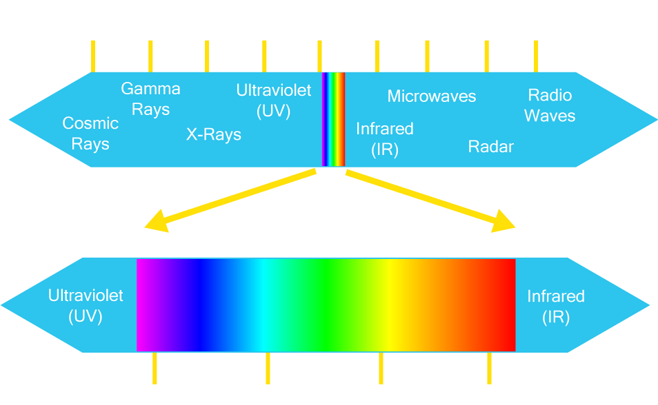
We’re all familiar with terms like Radio, Microwave, Light and X-Rays – these are all different frequencies of electromagnetic radiation. The light which we see with our eyes is just a small sliver of the electromagnetic spectrum, around 400-700 terahertz (THz).
Radio waves refer to frequencies in the KHz and GHz range, and include things like WiFi, BlueTooth, mobile phone communication, satellite communication, and of course FM radio.
Of course radio waves and communication are very useful, as per the above examples, however our electronic devices can also sometimes generate unintentional and unwanted radiation, which can interfere with other devices as well as their intentional communications. We don’t want our WiFi to stop working when the neighbour turns their microwave-oven on.
In extreme cases electromagnetic radiation can be weaponised, such as with the EMP (electro-magnetic pulse) produced by an electromagnetic bomb, or such as with radio jammers which intentionally disrupt communications.
In terms of our electronic devices, EMI (ElectroMagnetic Interference) and EMC (ElectroMagnetic Compatibility) refer to how nicely our devices behave with regards to electromagnetic radiation. Typically this refers to EM in the radio-wave range, since our electronic devices typically operate with clocking frequencies in the KHz, MHz and GHz ranges.
- EMI refers to unintended electromagnetic radiation emitted from our devices (which may interfere with other devices).
- EMC refers to how nicely our devices behave with regards to electromagnetic radiation.
In terms of EMC, we need to know that our important devices (medical equipment, vehicle engine-management-systems, etc) will still continue to operate properly even if they are exposed to a certain amount of unwanted electromagnetic interference.
In terms of EMI, note that all electronic devices with any switching of current will generate at least some level of electromagnetic radiation, however we need to keep these emissions below certain levels in order to comply with legislated standards.
Certification of Products
In order to obtain certification for our products, which may be requried in order to sell them in certain markets, it is usually required to pass an EMI/EMC test, which is carried out by certified test facilities. An EMI radiated emissions test may look something like the following:
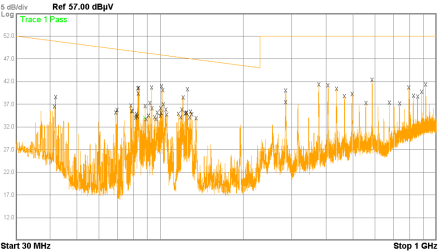 EMI Radiated Emissions Test Bode Plot.
This is a Bode Plot or frequency analysis graph where the horizontal axis represents frequency and the vertical axis represents magnitude – it shows the magnitude of emissions over a range of frequencies (see our Fourier Transform article). In order to pass the test, all emissions must be below the level indicated by the orange line at the top.
If an emission is above the specified limit then the device will not pass the test:
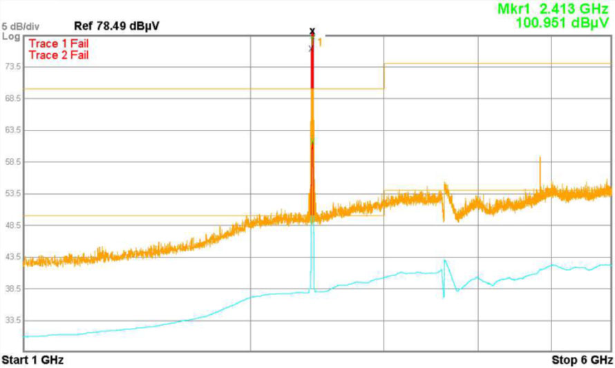 Emissions above limit - device fail.
Tests are conducted in a special test chamber, under standardised conditions:
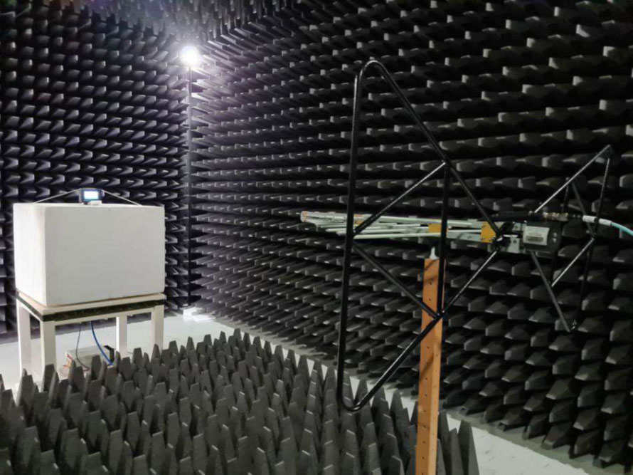 Chamber for device EMI testing.
An antenna picks up the radiations emitted from the device, and a spectrum analyser plots them on the graph.
Designing for EMI/EMC compliance is in a way the opposite of designing a radio. We want to make sure that our device is not a radio (at least not other than for where we specifically intend it to be at certain frequencies, such as if our device communicates via WiFi). As we all know, radios need antennas. Antennas emit electromagnetic radiation when an alternating current is connected to them (EMI), and generate voltage/current when electromagnetic radiation is received by them (EMC).
Technically, electromagnetic radiation is emitted by charged particles undergoing acceleration (which happens when current changes direction, or starts and stops). Designing for EMI/EMC requires attention to the AC (switching voltages/currents) components in our system, and the traces (wires) in our system which may be acting as antennas.
In general, implementing good high-speed design techniques (see our High Speed PCB Design Introduction article) will also help with EMI/EMC.
Return Currents
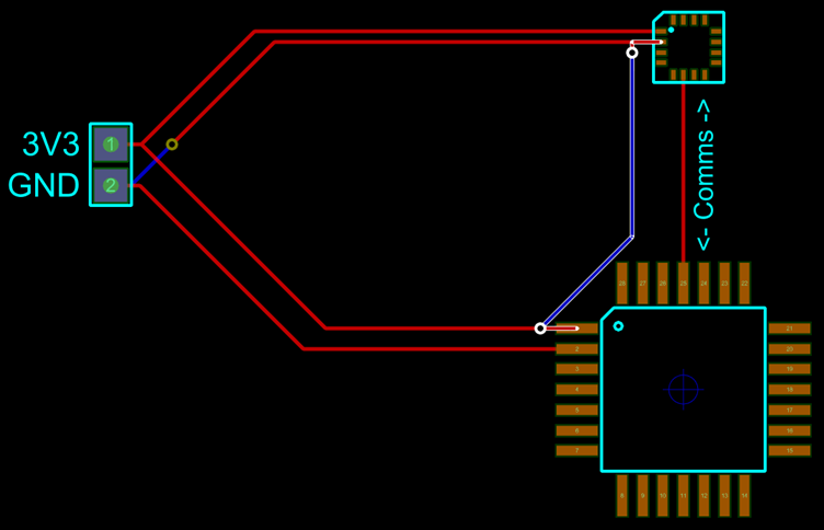
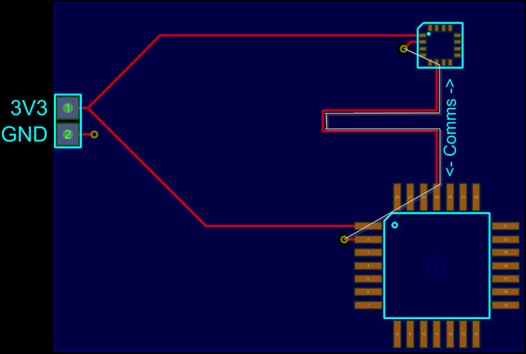
We may not think about it, but every signal on our board has to have a return path. Usually this is via a power net, such as Ground (GND). Consider the following scenario:
We have two devices communicating with each other on our board (say a microcontroller and a sensor). There is a relatively short comms line between them, and conceptually that is generally all we look at when we think of the communication between the devices; but there also has to be a return current for the communication line, and that comes via a power line, which may take a much longer route. Longer routes mean bigger antennas. When designing for EMI/EMC, we need to take the return current path (power line) into consideration as well and try keep this as short as possible (smaller antenna).
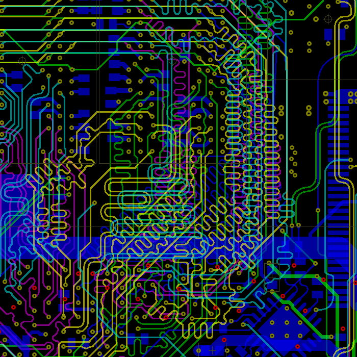
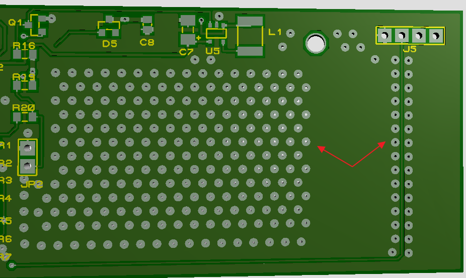
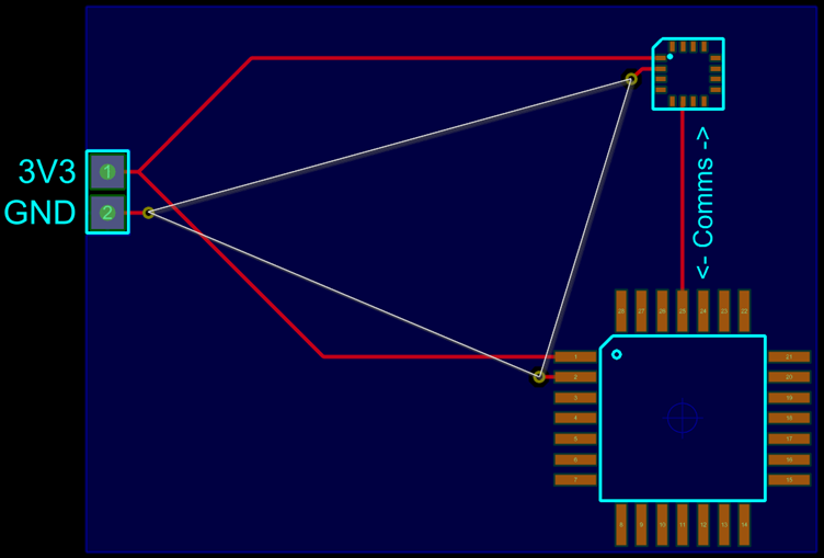
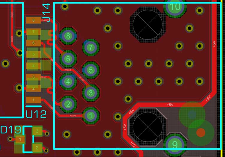
When implementing high-speed design principles, which generally involve 4-layer+ boards, we typically use inner layers as power-planes. By simply adding vias to the power-planes near our components, we can ensure short return paths for our currents (power-plane indicated in blue, white lines indicate conceptual current paths):
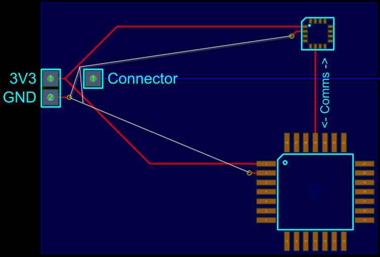
We should be careful to make sure that we don’t have breaks in our power-planes which may result in longer current paths again (again, white lines indicate conceptual current paths):
Again, this is inline with high-speed principles of ensuring constant impedance along high-speed lines.
Path-of-Least Impedance
Speaking of impedance; it is interesting to know that whilst direct currents (DC) follow the path of least resistance, alternating currents (AC) follow the path of least reactance (impedance). This makes sense, when we consider that reactance is the AC equivalent of resistance. If you’re not familiar with reactance/impedance, then please check our article on Passive Filters. As frequency increases, the inductive element of reactance plays a larger part, and currents essentially start to follow the path of least inductance. What this means, is that as frequency increases then currents will actually try follow directly underneath the relevant signal lines:
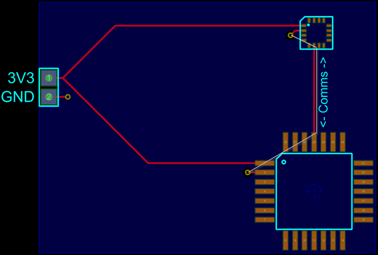
This is why it is important to maintain unbroken power-plane beneath high-frequency lines. Even if the signal line follows an odd path, the return current will still want to follow directly underneath it at higher frequencies:
Decoupling Capacitors
As the current demanded by the components on our board changes (for example, a CPU suddenly requiring more power to do complex calculations), the currents in the power-supply traces on our board will change as well – again turning these traces into antennas. By having sufficient decoupling capacitors on our board, as close as possible to the relevant components, we can reduce this as much as possible. Another way to look at this is that the decoupling capacitors provide a low-impedance path between power and ground for the alternating currents to flow through. You can read more about Decoupling Capacitors in this blog article.
Via Stitching
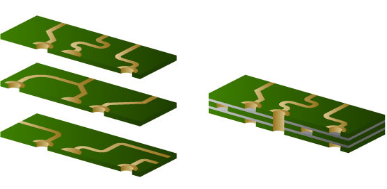
Via stitching refers to placing numerous vias connecting two (or more) power planes on different board layers.
Whilst we conceptually consider the power planes to be connected and the same even if they are only joined by a single via at the corner of the board, changing power demands and electromagnetic radiation may actually result in slightly different voltages between the two (or more) power planes. By placing stitching vias through the power planes, we can ensure that any voltage differences which may arise can be resolved via short current paths – again reducing the sizes of our antennas.
Slew Rates
Slew rate refers to how fast a signal rises or falls. We may conceptually think of voltage levels changing instantaneously, but this is never the case – it always takes some finite amount of time for the voltage to transition from one level to another. Very fast transitions result in more acceleration of charged particles over a short period of time and therefore higher electromagnetic radiation emissions. Another way to look at this is that, in terms of a fourier transform (see our Fourier Transform article), the more square the edge of a signal is the more high-frequency components it contains. Some microcontrollers have adjustable slew rates for this reason, to slow down the speed of signal transitions and reduce the squareness of the signal edges. Reducing slew rate (within the limits of the speed required for the actual required signal frequency - we can’t have a 1ns slew on a 1GHz signal, since the frequency period of 1GHz is 1ns) can reduce electromagnetic radiation emissions.
Staggering
Some ICs with wide communication buses may include an option to stagger the switching of individual lines within the bus. Staggering the switching, instead of switching all the lines at once, can help spread the resulting EMI out across time and thus reduce the total EMI at any given moment to within acceptable levels.
Shielding
Shielding is often the first solution thought of in terms of EMI/EMC, but really it should usually be the last consideration after the above points have been addressed. Signals can escape from even small gaps, such as the side of a PCB, and shielding can sometimes be the equivalent of trying to fix a mechanical product with copious amounts of duct-tape. That said, shielding does have its place – it just shouldn’t be the go-to solution without ensuring proper PCB design first.
Watch how to automatically apply shielding or full stitching in Proteus in this video.
Summary
Designing for EMI/EMC involves considering the AC (switching) components of our system and taking steps to reduce the size of current loops. Usually, a design which has been done with high-speed design principles in mind will also have good EMI/EMC. Principles such as ensuring unbroken power-planes under high-speed tracks, good use of decoupling capacitors, vias to power-planes around switching ICs, and generally trying to keep high-frequency tracks relatively short if possible, will help with EMI/EMC. DC-DC converter circuits, for example, should be as small and tight as possible, with good decoupling capacitors nearby. A 2-layer design which is failing EMI/EMC may get a pass simply by changing to 4-layer with ground planes on the inner layers and stitching vias near ICs. Further steps which can be taken include looking at which specific frequencies are being generated by the board and tracking down what the source might be, using tools such as near-field probes to pinpoint sources of emission, using TEM cells for quick pre-certification tests and to see the results of hardware and software changes, and using other EM analysis tools such as EM scanners; these may be the subject of a separate article.
All content Copyright Labcenter Electronics Ltd. 2026. Please acknowledge Labcenter copyright on any translation and provide a link to the source content on www.labcenter.com with any usage.Get our articles in your inbox
Never miss a blog article with our mailchimp emails