Introduction
Operational Amplifiers, or “Op Amps”, have 5 main connections:
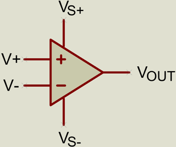
VS+ and VS- are called the power rails and supply power to the opamp. Conceptually, VOUT can output a voltage anywhere between VS+ and VS-; in practice it is limited to a little less than VS+ / more than VS- , depending on the particular opamp and depending on the load (how much current is drawn from the opamp). This is due to the voltage drops over the internal transistors.
V+ and V- are the inputs to the op-amp, and are differential meaning that the opamp works on the difference in value between these two inputs. As the name implies, the opamp amplifies (multiplies) the differential input before passing it to the output. The multiplication value, or gain, is very high – around 100,000x for most opamps – however techniques can be used to make the opamp have a more reasonable gain (such as 2x or 10x, for example), as we will see in the following sections. V+ is also called the non-inverting input, and V- the inverting input.
The Comparator
A comparator is a device which compares two analogue voltages and then produces a binary digital output (high or low, 1 or 0, true or false) depending on which voltage is higher. Put another way, the comparator answers the question: Is V+ higher than V-?
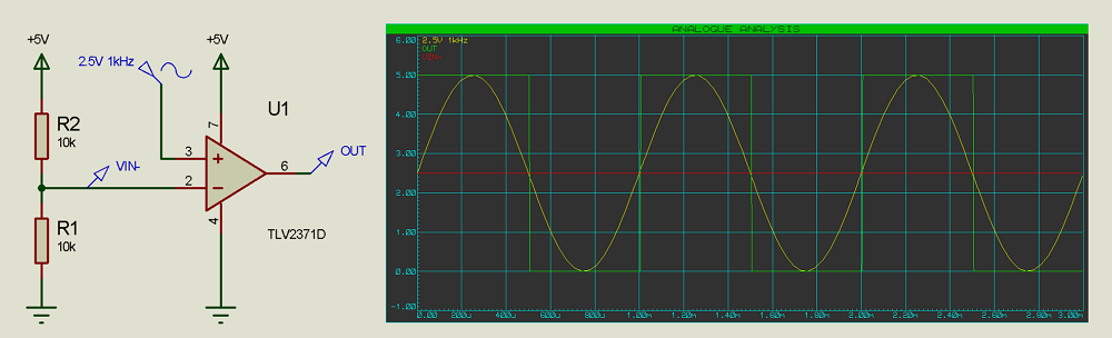
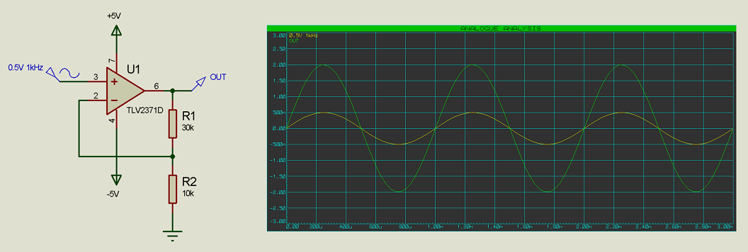
In the above example we have connected the positive supply of the opamp to +5V and the negative supply to 0V (GND). V- is supplied with a +2.5V reference from a voltage divider (resistors R1 and R2). The opamp is asking the question, Is V+ greater than 2.5V?
When V+ (yellow trace) goes above 2.5V (red trace) then the output (green trace) goes high/true (+5V), and when V- goes below 2.5V then the output goes low/false (0V/GND).
By changing the value at V-, we can change the question – for example, Is V+ greater than 1V?

The Buffer
Opamp inputs are high impedance, meaning that they do not draw relatively much current. This is especially important when the source signal supplied to the opamp is also high-impedance, meaning that it cannot supply much current, because otherwise the signal would be distorted as the current drawn by the opamp or load pulled the voltage down.
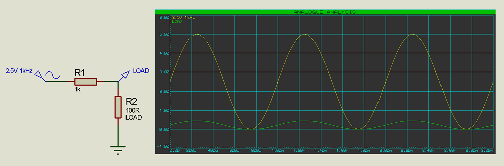
In the above example, the input to the load is high-impedance (1k resistor limiting the current which can be supplied). As a result, the signal (yellow trace) is severely distorted (green trace) by the time it reaches the load.
By feeding the output of the opamp back into V-, we can give the opamp a gain (multiplier) of 1 (unity), and the opamp will supply additional current from its power rails (low impedance).
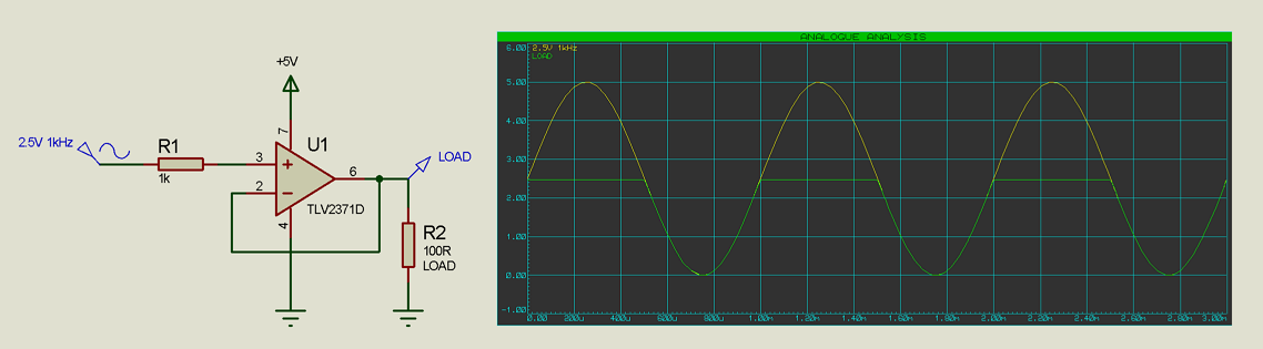
Due to the voltage drop over the internal components making up the opamp, we are seeing that it can supply a maximum of about 2.5V at the output with this load however, which we can solve by supplying the opamp with +9V on the positive supply:
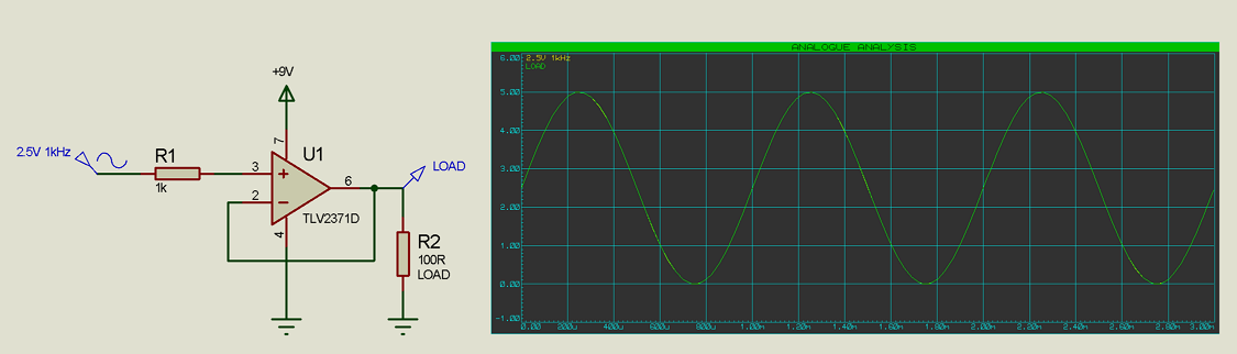
By using the opamp in buffer configuration, and supplying it with enough power/voltage, we can convert the high-impedance source to a low-impedance output.
To understand the mechanism of how the buffer configuration works, consider the following 3 scenarios (remembering that the output and V- are linked):
- Positive Differential Output
- Negative Differential Output
- Zero Differential Output
V+ > V-. The opamp multiplies the difference and increases the output voltage, thus also increasing the voltage at V- and decreasing the size of the differential input.
V+ < V-. The opamp multiplies the difference and decreases the output voltage, thus also decreasing the voltage at V- and again decreasing the size of the differential input.
V+ = V-. The opamp output stays the same.
What we can see is that the opamp will always adjust the output / V- in order to decrease the differential input, until the output matches the V+ input and stabilises. Another term for this is that the output tracks the V+ input.
The Amplifier
Finally, we get to the namesake implementation of the operational amplifier – actual amplification. By scaling the feedback to the V- input, we can get a gain (multiplier) of something other than 1 on the output.
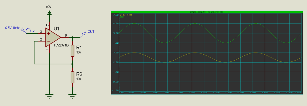
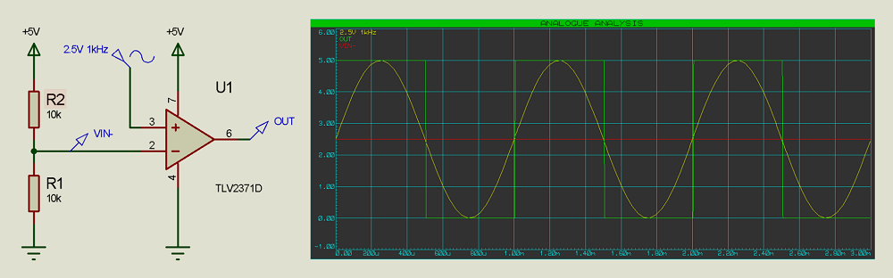
In the above example, we have a 0.5V 1kHz sine wave input which is centred around 2.5V. Note that we are also again providing +9V to the positive supply. There is a 1:1 ratio on the voltage divider which is feeding back to the V- input, resulting in a gain of 2. The output might not be exactly what you were expecting, because it is centred around 5V, but technically this is correct – all the voltages have been multiplied by 2. The 2.5V centre becomes 5V, the 3V peak becomes 6V and the 2V trough becomes 4V (1V peak-to-peak amplitude between 2V-3V multiplied to a 2V peak-to-peak amplitude between 4V-6V).
If we want to select 2.5V as our centre (or offset) voltage for the amplification, then we must reference our gain feedback to +2.5V (which could potentially be supplied by a separate buffer opamp if necessary):
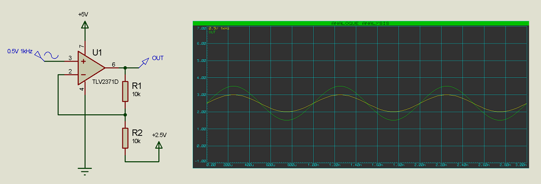
Now our peaks are at 3.5V and our troughs at 1.5V, which still gives a peak-to-peak amplitude of 2V (and therefore gain of 2x).
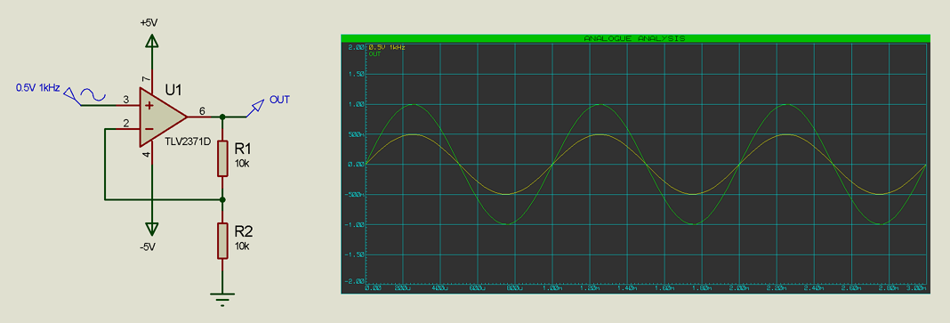
Of course, we can also have inputs and outputs centered around 0V, by supplying the negative power rail of the opamp with a negative voltage (and of course supplying an input signal centered around 0V to the V+ input):
By changing the ratio on the feedback voltage divider we can change the gain, such as the below 3:1 voltage divider which results in 4x gain:
Comparator with Hysteresis (Schmitt Trigger)
Hysteresis can be described as a reluctance to change. Hysteresis essentially says, once I’ve changed, it will take some persuasion to get me to change again. This can be very useful in order to prevent an output from flip-flopping (changing rapidly) when an input is hovering around a threshold. For example, we might have a fan which turns on when the temperature gets above 30°C; we may find that, as soon as the fan turns on then the temperature drops to just below 30°C (say to 29.99°C), resulting in the fan switching off again – as soon as the fan turns off then the temperature rises back to 30°C again, and the fan turns on again. This cycle could repeat very rapidly, which would be both probably damaging to the fan motor and annoying to any people nearby. Adding hysteresis to this system would mean something like saying: The fan turns on when the temperature reaches 31°C, but it may not turn off again until the temperature has dropped to below 29°C.
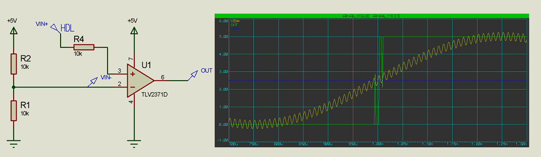
Hysteresis can be added to a comparator opamp configuration by feeding the output back to the V+ input:
In this case we can see that the output hesitates to change after the 2.5V threshold until the input has exceeded it by approximately another 1V.
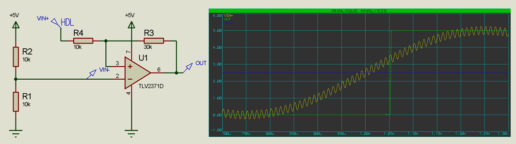
By adding some noise to the input, we can see the usefulness of hysteresis:
In the above circuit, the output switches on and off rapidly as the noisy input crosses the threshold.
With hysteresis added, we get a clean single switch:
Opamp Specifications
Of course, there are many different models of opamp available, varying in specifications and cost. Some of the specifications include how quickly the opamp reacts to changes in input (bandwidth, which will determine the maximum frequency which the opamp can handle), the maximum voltages which the opamp can work with, how closely the output can match the supply voltages (rails), how much current the opamp can output, and so on; parametric search on supplier websites, and datasheet examination, will aid in selecting the correct opamp for a particular application.
Conclusion
Operational Amplifiers are an important building block in analogue signal processing circuits, and also find use as comparators in digital applications.
Proteus provides a number of tools and sample designs for designing and testing opamp circuits, including both static graph-based analysis and real-time interactive simulation. The 741 Noise Analysis Sample features a 741 OpAmp drawn entirely from the internal components comprising the integrated circuit, which allows for additional detailed analysis.
All of the test cases and graphs in this article were created with the Proteus Design Suite. The Advanced Simulation Features module provides over a dozen different graph types and easy access to signal generators and voltage/current probes.
All content Copyright Labcenter Electronics Ltd. 2026. Please acknowledge Labcenter copyright on any translation and provide a link to the source content on www.labcenter.com with any usage.Get our articles in your inbox
Never miss a blog article with our mailchimp emails
Embedded Simulation
Learn more about our world leading embedded simulation, Proteus VSM. Simulate and debug your microcontroller firmware on the schematic alongside all the analog and digital peripherals connected to it.
 Ask An Expert
Have a Question? Ask one of Labcenters' expert technical team directly.